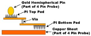
Basis of Particle Interconnect technology
|
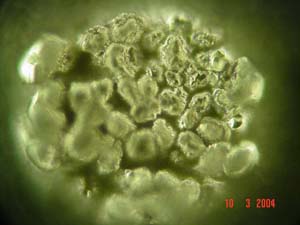
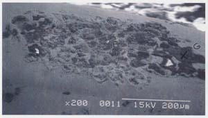
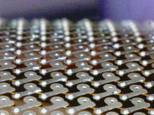
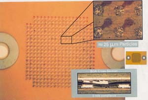
Close-up of Particle Interconnect pads shows controlled stacking of particles to a desired height with clearance between individual particles. |
"Particle Interconnect" (PI) overview
Description
Particle Interconnect replaces soldering, wire bonding, and on-bump bonding with environmentally safe, diffusion bonding at very low contact force, and no wiping.
Bonding temperature can vary from -270° C to > 450° C, allowing to minimize thermal stress due to CTE mismatch. Mono-metallic bonds (Particle Interconnect) unlike bi-metallic ones (solder) do not decay over time, due to temperature.
Particle Interconnect is the ultimate technology in electrical / mechanical / thermal interconnection with best price and best performance (not just price/performance) compared to other interconnect technologies.
Particle Interconnect is the only interconnect method with lead length of 0.001" (25 μ), bandwidth > 100 GHz, and a lifetime of > 1.5 million insertions, with extreme acceleration tolerance.
This unique technology creates an oxide penetrating, non-wiping gas tight connection that allows electrical connection in presence of adhesive, oil, and dirt.
Eliminating wirebonding, PCB drilling, and reducing PCB blind vias leads to device miniaturization by more than an order of magnitude, with reduced power needs and costs, through the use of MCM or SIP.
Because of reduced process steps and reduced material costs, the interconnect cost half the current industry practices. Additionally, mounting these connection points is faster, easier, and requires little specialized equipment or skilled labor.
Usage
All steps of electronic product development: prototyping, test (controlled impedance), burn-in, emulation/characterization, field replacable, and production. Particle Interconnect technology reduce costs of burn-in die before assembly (KGD).
Particle Interconnect provides rugged miniature interconnects for integrated circuit die, packaged devices, low-cost probe cards, and test fixtures.
Since bond strength is a function of contact force (it determines contact area), one can:
- Test the final product without testing individual parts. Since defective parts can be easily replaced.
- Repair and upgrade the system in the field.
- Rapidly disassemble and reuse or recycle electronic components.
Anti-stiction coating for MEMS, since particles do not wear out.
Features
- Temporary, or permanent contact even in presence of adhesive, grease, or solder.
- Minimal disturbance of contact mating surface.
- Simple mechanical connection and trace design.
- Gas-tight oxide-penetrating connection.
- Plastic deformation of contact mating surface.
- Independent of common electronic metals.
- Contact material: nickel, gold, copper, ...
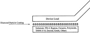
- Substrate material: polyimide, FR-4, ceramic, ...
- Temperature range used: > 450° C; to -270° C.
- Minimum interconnect dimensions: 6 μ pad, 12 μ pitch.
- Attached die passed four cycles of Mil-Std-883C (burn-in, thermal shock, pressure, salt/fog corrosion) test without any damage.
- No lead, see: U.S. Environmental Protection Agency - Design for the Environment (DfE) - Solders in Electronics: A Life-Cycle Assessment
- Life test: at 30 gram-force produced 3 - 5 milli-Ohms contact resistance even after 1,500,000 insertions, because metal matrix binding the particles is elastic and does not creep.
- Contact force & resistance:
- 10 gram-force, 10 milli-Ohms of resistance,
- 50 gram-force, 3 milli-Ohms of resistance.
- Current carrying capability: 0.020"2 pad at 9 gram-force has > 12 amps.
- Vertical axis contact length (signal integrity requires small size): 0.001" (25 μ).
- Vertical axis compliance (accomodating non-planar die): > 0.040" (depending on design).
- Method for penetrating the oxide of package lead: sharp small diamond particles with no scrubbing for durability, compared to metal scrubbing or metal penetrating contacts.
- Controlled impedance: 50 Ω ± 1 Ω to the lead of package (Typical design capacitance & inductance: < 0.001 pF & < 0.01 nH).
- Bandwith tested to > 65 GHz (for high-speed and radio-frequency applications).
- All steps of electronic product development: prototyping, test (controlled impedance), burn-in, emulation/characterization, field replacable, and production.
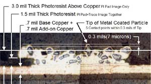
Physical description
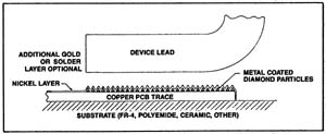
| Particle Interconnect uses sharp, metallized, particles which have been screened by size. They are attached onto contact pads on the surface of conductor using standard masking and electroplating processes. The sharp, embedded particles create a "micro bed-of-nails" of "conductive sandpaper" that makes many parallel electrical paths by penetrating through any oxide without requiring a wiping action as conventional contacts. This non-wiping action, oxide penetrating patented process is capable of penetrating surface contamination, oils, and create a gas-tight electrical contact. | 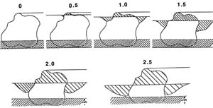 |
| Particle size | Pad size diameter | Penetration |
| 10 μ ± 2 μ | < 0.005" | small |
| 25 μ ± 5 μ | 0.005" to 0.100" | medium |
| 125 μ ± 10 μ | > 0.100" | large |
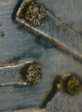
Cross-section of Particle Interconnect pad
Following picture demonstrates uniformity & planarity of particle protrusion above photoresist.
- 0.020" (500 μ) diameter x 0.003" (75 μ) tall nickel Particle Interconnect pad on 1 oz copper.
- Using 25 μ particles. Planarity of 1/2 particle diameter.
 |
 |
Picture courtesy of Larry DiFrancesco. |
Particle Interconnect planarity and accuracy
Following picture demonstrates planarity of pads and accuracy of alignment of particles on pads.
 |
 |
| PCB traces with pads | Close up |
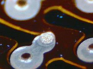
Note sharp corners of the particles that make electrical contact at very low pressure to form a temporary bond. Solder would wick into spaces between the particles during reflowing to form perament bond.
 |
|
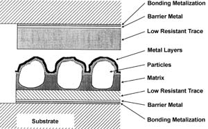
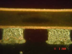
| Cross-section of the Particle Interconnect (PI) pad shows planarity of a single pad as well as planarity to adjacent pad. | Close-up of PI pads shows controlled stacking of particles to a desired height with clearance between individual particles. |
Electrical performance
The Particle Interconnect joint formed by pressing particles through the metal oxides into the lead has electrical stability and performances superior to a solder joint. Contact resistance is extremely low, measuring 3 - 5 milli-Ohms, and does not change even after 1.5 Million remates.
Particle Interconnect technology received an endorsement from Hewlett-Packard, Microwave Division for the excellent high frequency (> 20 GHz) performance they obtained when testing high frequency IC parts.
The contaminates and oxides present on metal contact surfaces mandate the wiping action to make reliable electrical connection. The wiping action high compressive forces cause plastic deformation of the contact surface thus exposing the clean metal surface beneath.
Work performed by different research groups indicates that the electrical connections are made through the asperities present on the electrical surface. Equations were developed by one research consortium which indicate there is a relationship between contact-resistance, contact-force, the number of asperities, the size of the asperity, and the asperities distribution.
Particle Interconnect technology forms a contacting surface that has a large number of asperities. These asperities have very sharp and hard points due to the nature of the particle or crystal used (e.g., diamond). The sharp points do not dull or wear since the crystal is much harder than the opposing metal surface.
A key feature of Particle Interconnect technology is the use of many parallel connections. The Particle Interconnect surface is like conductive sandpaper and like sandpaper has many points to penetrate any opposing surface. The Particle Interconnect surface is also similar to a micro-bed-of-nails. Like the bed-of-nails, the Particle Interconnect surface has many parallel paths for contact reliability and durability; a long cycle life; high current capacity; very low contact resistance; and forms a gas-tight joint for better performance in harsh dynamic environments.
The Particle Interconnect joint is a pressure only connection which requires no sliding or wiping action. Thus the connection is not an element in the electrical chain, but is a matched impedance connection. With no impedance mismatch, there is no reflected energy. Reducing the amplitude of the reflected signal allows for faster signal transmission with greater signal fidelity.
Low contact force requirement
Sharp particles in Particle Interconnect concentrate contact force into a very small area. The high pressure pierces oxides and other contaminants on surfaces without requiring large amounts of force on the contact. Reliable, gas-tight connections can be made with Particle Interconnect with as little as 10 grams of force per contact. This low level of force is enough to drive the particles into the mating surface and provide a contact resistance of 3 to 5 milli-Ohms.
Re-mateability
Insertions of the particles do very little damage to the mating surface. This provides very long re-mate life with very little degradation of the connection. Since there is no wiping action, contact coatings stay intact. Connection tests against standard solder balls have proven a life of over 30,000 insertions with no significant damage to the contact's performance.
Material compliance
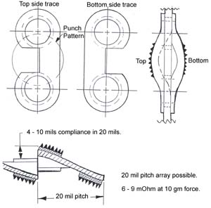
These particles can be applied to many different substrates - flexible, rigid, metallic, and non-metallic.
This ability coupled with the very low contact force gives us the capability to make very reliable interposers with large compliances out of materials that would collapse if exposed to the normally required contact forces. Compliances from 0.002" to 0.020" result.
Controlled impedance to lead of package / die pad
Controlled impedance to lead of package
 |
 |
| Schematic for controlled impedance socket. | Surface of PLCC J-Lead after 30,000 insertions. Surface finish of lead passed steam aging test. |
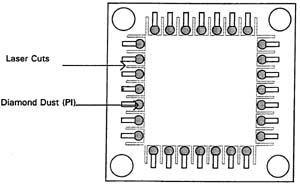
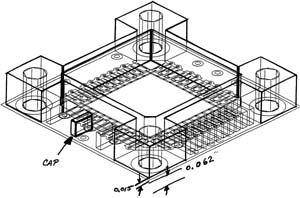
Controlled impedance socket
44 pin controlled impedance Particle Interconnect PLCC socket or interposer with singulate leads. Decoupling capacitors are within 0.100" of PLCC pad.
 |
 |
| Printed circuit board layout | Mechanical hold down |
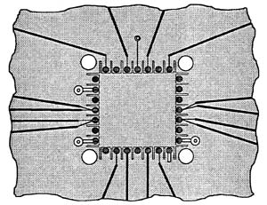
Circuit layout for controlled impedance socket
D.U.T. board layout use for TDR measurement. The traces are narrowed to compensate for Z0 change due to devices present in the socket.
 |
 |
TDR of controlled impedance Particle Interconnect socket (interposer) on load board
 |
 |
||||||||||||||||||||||||||||||
|
|
||||||||||||||||||||||||||||||
|
|||||||||||||||||||||||||||||||
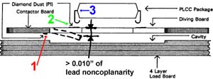
- Cursor at contact point on diamond dust/diving board with no part in socket.
- Trigger is continuously running at 10.0 kHz with step on.
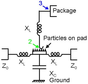
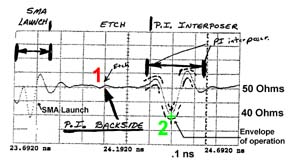
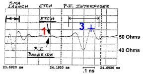
- Demonstrated controlled impedance connector from contactor board to mother board using Particle Interconnect with impedance tolerance of 50 Ω ± 1 Ω.
- Controlled impedance of J-lead going to package.
- Compensation (Point 2 on graph) to neutralize internal inductance and capacitance of PLCC package (Point 3 on graph).
- Particle Interconnect is 10 times better than SMA connector (Point 1 on graph).
- Additional work by MMS, TI, and HP.
Diamond Particle Interconnect interposer vs. solder ball
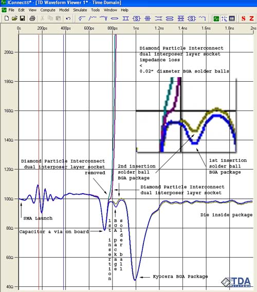
TDR data illustrates zero reactance and consistency of Diamond Particle Interconnect socket compared to soldered connection and SMA connector.
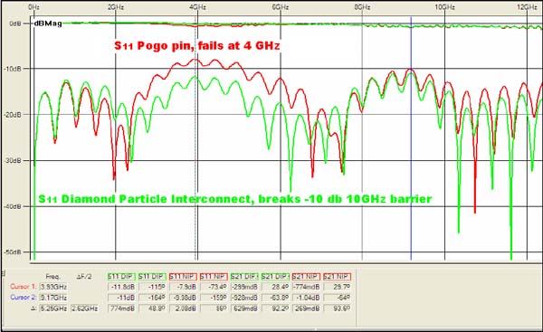
Particle Interconnect vs. pogo pin S11 parameters
The measured insertion and return loss shows a 4 GHz resonance at the solder ball causing PCI-X return loss failure below 6 GHZ. By replacing the standard pogo pin socket with Particle Interconnect socket the return and insertion was measured beyond 12 GHz, without modifying the board.
Particle Interconnect contact resistance vs. contact force
Gold probe to top side Particle Interconnect
Particle Interconnect's very low resistance results in higher current capacity.
- 1 mm pitch BGA interposer.
- 9.2 grams contact force (.0902 N, .020 lbs, or .325 Oz.), 12 amps.
- Contact resistance = .00433 Ω
 |
 |
| Particle Interconnect array top side | Particle Interconnect bottom side close up |
Features comparison
Electrical performance
| Lead Type | pF | nH |
| SMD | 1.0 | 1 - 12 |
| Pin Grid Array (PGA) | 1.0 | 2 - 5 |
| Wire bond | 0.5 | 1 - 3 |
| Solder bump | 0.1 | 0.01 |
| Particle Interconnect | < 0.001 | < 0.01 |
Reflow solder bump vs. Particle Interconnect
| Reflow solder bump | Particle Interconnect |
|
• Select limited number of untested chip(s)
• Solder bumped chip to substrate • Clean substrate & chip • Apply adhesive (chip underfill) • Cure adhesive (sealing chip-substrate) |
• Select test/burn-in unlimited number of chip(s)
• Attach chip to substrate at room temperature • -- • -- • -- |
Database for solder properties with emphasis on new lead-free solders
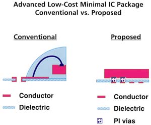
Particle Interconnect trace/via process vs. conventional PCB package
Less steps = less costs.
| Conventional | Particle Interconnect |
|
|
Particle Interconnect features vs. lead frame and BGA arrays
| User Feature / benefit | Lead frame | BGA arrays | PI | Notes |
| Low cost | Yes | No | Yes | Particle Interconnect imposes no penalty for close pitch high lead count. Initial costs 0.5 cents/pin in high quantity. |
| Reliability | Moderate | High | High | Particle Interconnect is gas tight and redundant. |
| Fluxless solder reflow | No | No | Yes | |
| Economically eliminate lead metal | No | No | Yes | Solder is no longer needed for electrical attachment. |
| Controlled impedance possible | No | Sort of | Yes | Particle Interconnect substrates can easily be multiple layers. | Array die pad attachment | No | Yes | Yes | Extremely low Z for IC power attachment | No | No | Yes | Die attach sites can be any length and shape. | Low initial capital requirements | Yes | No | Yes | Particle Interconnect infrastructure consists of enhanced PCB production facilities. | Rapid low cost custom lead frames | No | No | Yes | PCB turn around times. | Significant future cost reductions | No | No | Yes | Initial PI per pin costs are significantly higher than estimated processing and material costs. | Multiple temperature Silicon attach | No | No | Yes | Enables improvements in support services. Board test, burn in, wafer test, high density final test points for assembled boards, membrane probes for IC's, etc. | No | No | Yes | Radically lower electrical parasitics possible. True Z axis rematable connection at low applied force. Broad implications at every level of interconnect. | Enabling technology for MCM | No | Yes | Yes | Enables bare die testing. Chips can be replaced if failure occurs during final test. |
Applications
Contactor sockets
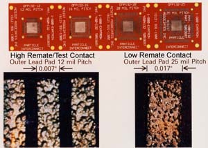
Particle Interconnect is used as interconnect between surface mount devices, load boards, testers, programmers, and other repeat-insertion applications. With a total interconnect between device under test (DUT) lead and test circuit trace of less than 0.001".
The typical resistance of a conventional test socket begins at approximately 30 milli-Ohms. As a conventional test socket begins to wear out, the contact resistance begins to increase and contact resistances of over several hundred milli-Ohms are common. By the time a conventional test socket receives 10,000 insertions, it can begin to fail in exacting test applications.
The Particle Interconnect begins with 3 milli-Ohms of contact resistance, and is still 3 milli-Ohms after 1,000,000 insertions on a rigid board and 100,000 insertions on a flex board.
Ultra high frequency sockets
A common problem encountered in high-frequency test fixtures is the impedance mismatch between the device under test and the test circuitry. This mismatch is typically caused by the use of a conventional test socket or contactor assembly. A conventional test socket has built-in resistance. Due to its physical characteristics, it forces the test circuitry to be placed a minimum distance from the device under test. All of these factors contribute to increased resistance (R), capacitance (C), and inductance (L).
However, due to the superior physical characteristics of Particle Interconnect (PI), and because Particle Interconnect contacts exhibit the same electrical characteristics as a solder connection, use of Particle Interconnect can effectively eliminate the impedance mismatch of conventional contactor assemblies.
Printed circuit boards
PCBs can be made from rigid or flex specialty dielectric substrates, or etched BeCu.
Interposers
 |
 |
One valuable use of Particle Interconnect coating is in interposers. Whether part of a BGA socket, connecting two PCBs or joining many other connectors. Three characteristics make this technique work: very low contact force, excellent re-mateability, and ability to apply Particle Interconnect to a variety of surfaces.
Sample products
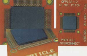
Particle Interconnect Package (PIP)
Advanced low-cost minimal IC package.
 |
 |
| QFP 132 lead, 0.012" pitch OLB (Outer Lead Bond). | Leadframe / Chip-On-Board socket & carrier. |
|
 |
Particle Interconnect lead frame package
 |
 |
| Solder bumped chip (ILB) on Particle Interconnect lead frame (OLB). | Particle Interconnect bumped chip (ILB) on Particle Interconnect lead frame (OLB). |
Particle Interconnect surface mount BGA socket
 |
 |
| 0.030" pitch 19x19 miniBGA. | 0.050" pitch, 15x15 through-hole BGA socket. |
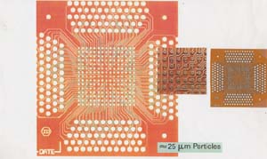
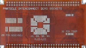
Demo sockets
One lead in each socket is deliberately removed, in order to prevent its use as an actual production socket.
 |
 |
| 28 pin SOIC/SOJ; 20, 28, 32, 44 PLCC/LCC; 32 pin TSOP. |
Particle Interconnect contact detail. |
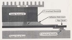
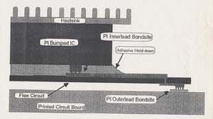
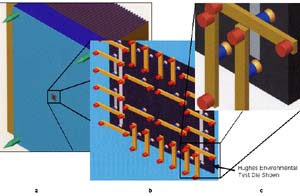
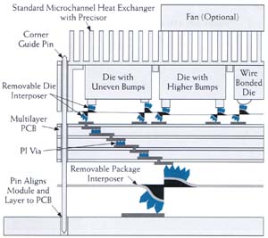
Removable die Multichip Module - L/D/C
|
|
 |
 |
| Removable die MCM | Louver contact |
- Low-cost heat exchanger designed for modular dissipation needs.
- Removable die locator (precisor) aligns all die on 0.010" edge-to-edge mosaic tile pattern of silicon.
- Precisor is accurately aligned by corner guide pins in heat sink.
- Removable die PI interposer sockets die to PCB and spring loads die against heat sink.
- Interposer is accurately aligned by corner guide pins in heat sink.
- Removable die PI interposers with 0.001" - 0.008" travel on 0.001" - 0.030" pitch are available.
- Removable multilayer PCB interconnects all die together with controlled impedance from die pad to die to pad.
- PI vias between laminate layers allow 0.002" "blind" vias by punching through adhesive layer during lamination.
- PCB is accurately aligned by corner guide pins in heat sink.
- Removable package PI interposer sockets package to PCB and spring loads package to PCB.
- MCM is accurately aligned and held to PCB by corner guide pins for manual or automatic insertion.
- Package interposers with 0.08"-0.020" travel on 0.010"-0.050" pitch with either peripheral or array patterns available.
- Die are removable by simply unstacking layers.
- Both bumped and wire bond die pads are mixable.
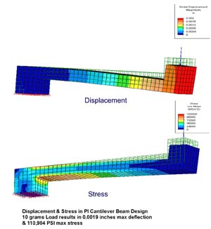
FEM analysis
PI cantilever displacement & stress
0.040" beam.
 |
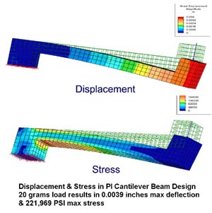 |
| 10 grams load. | 20 grams load. |