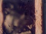
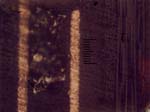
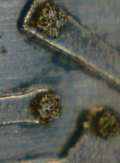
Optical Microscope pictures of PI
Particle Interconnect via
Connecting two conducting surfaces together.
| Particle closeup | Connector closeup |
 |
 |
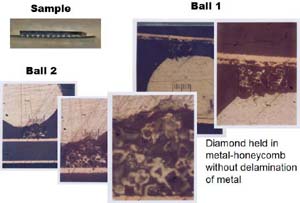
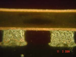
Particle Interconnect piercing SDRAM DDR1 package balls
- Demonstrating damage free performance when exposed to excessive loading.
- 60 pounds of force on 60 balls.
- Note minor depth of penetration.
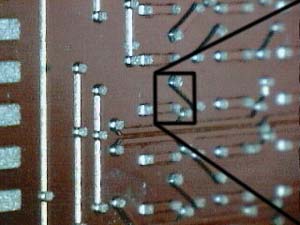
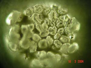
Particle Interconnect planarity and accuracy
Following picture demonstrates planarity of pads and accuracy of alignment of particles on pads.
 |
 |
| PCB traces with pads | Close up |
Note sharp corners of the particles that make electrical contact at very low pressure to form a temparory bond. Solder would wick into spaces between the particles during reflowing to form perament bond.
 |
 |
| Cross-section of the Particle Interconnect (PI) pad shows planarity of a single pad as well as planarity to adjacent pad. | Close-up of PI pads shows controlled stacking of particles to a desired height with clearance between individual particles. |
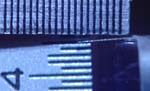
Beam bent against ball
Magnified 200X.
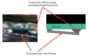
Beam bending
Travel/length is 30%.
 |
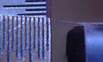 |
| 0.001" thick x 0.008" wide x 0.008" long beam | Beam bent once 0.020" down and once 0.025" up |