SEM, FIB, AFM pictures of metal
Focused Ion Beam (FIB), and Electron beam images of ultrahigh fine grain electroplated nickel.
Ion beam damage and redeposition products can be seen in these images, but ultrafine grain structure can not be seen even at 50,000x magnification.
Pictures are taken using FEI Strata™ DB235 courtesy of Richard Chin of Material Science and Engineering department at Stanford University.
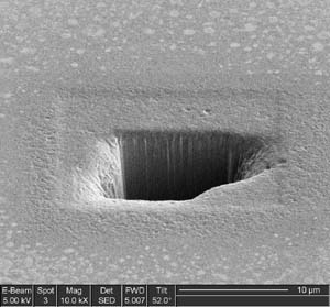
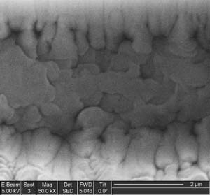
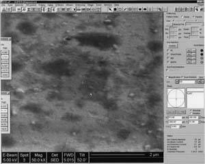
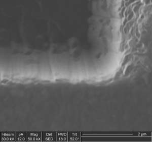
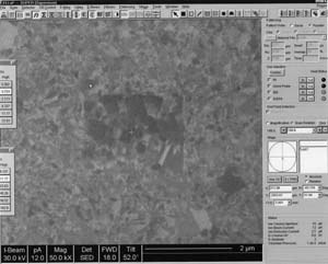
SEM
Hole etched by ion beam
Electron beam spot size is 3, chamber pressure is 10-5mbar.
FWD is Free Working Distance.
 |
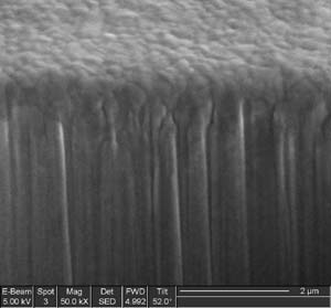 |
| (a) Oblique View of hole | (b) Wall of hole |
| 10,000x, tilted 52 °, FWD = 5.007 mm | 50,000x, tilted 52 °, FWD = 4.992 mm |
 |
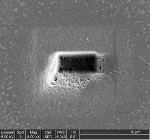 |
| (c) Bottom of hole | (d) Top view of hole |
| 50,000x, FWD = 5.043 mm | 8,000x, FWD = 5.043 mm |
Thin film
Electron beam spot size is 3, tilted 52 °.
FWD is Free Working Distance.
 |
| (a) Cross section |
| 1,000x, FWD = 5.447 mm, chamber pressure = 1.5x10⁻⁵mbar |
 |
 |
| (b) Surface | (c) Surface |
| 50,000x, FWD = 5.447 mm, chamber pressure = 1.8x10⁻⁵mbar |
50,000x, FWD = 5.015 mm, chamber pressure = 1.2x10⁻⁵mbar |
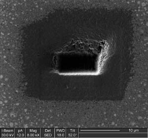
FIB
Hole etched by ion beam
Ion beam current = 12 pA, tilted 52 °, Free Working Distance (FWD) is 18.0 mm.
 |
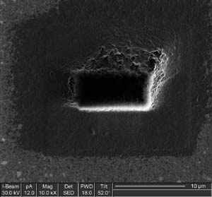 |
| (a) Oblique view of hole | (b) Oblique view of hole |
| 8,000x, chamber pressure = 10-5mbar | 10,000x, chamber pressure = 10-5mbar |
 |
| (c) Corner of hole |
| 50,000x, chamber pressure = 8.8x10⁻⁶mbar |
Thin film
Ion beam current is 12 pA, tilted 52 °, Free Working Distance (FWD) is 18.0 mm.
 |
| (a) Surface |
| 50,000x, chamber pressure = 1.2x10⁻⁵mbar |
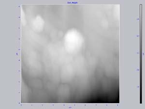
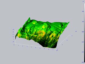
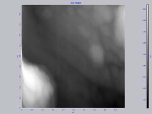
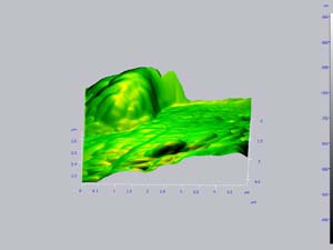
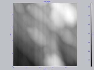
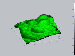
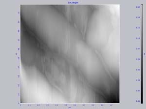
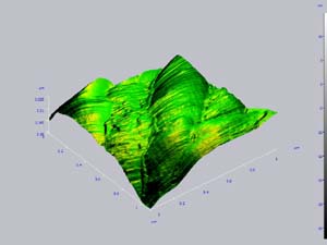
Atomic Force Microscope (AFM)
Cross Section
Pictures were taken using tapping mode on a NT-MDT instrument courtesy of Kim Kangasniemi of NT-America.
Gray scale color represent height.
 |
 |
| (x, y) = (9, 9) micron | (x, y, z) = (9, 9, 2.65) micron |
 |
 |
| (x, y) = (4.5, 4.5) micron rotated 90 ° | (x, y, z) = (4.5, 4.5, 2.6) micron |
 |
 |
| (x, y) = (2, 2) micron | (x, y, z) = (2, 2, 2.38) micron |
 |
 |
| (x, y) = (1, 1) micron | (x, y, z) = (1, 1, 3.225) micron |
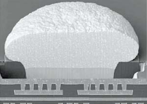
Lead free solder comparison
www.semitool.com/pdf_files/SEMITOOL_ECD_WLP_LOWCOST_MANUSCRIPT_FINAL.PDF
Low Cost, High Reliability Electroplating WLP Technology Integration of SnAg chip to chip interconnect
A survey of cost effective electroplating lead free bumps
 |
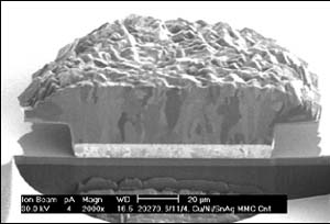 |
| Plated Sn Pb | Plated Sn Ag |