Surface Mount Package Test Fixture
Theory
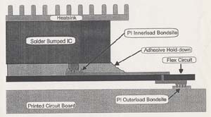
Testing bumped chip on Particle Interconnect leadframe
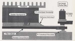
Controlled impedance to lead of package / die pad
Controlled impedance to lead of package
 |
 |
| Schematic for controlled impedance socket. | Surface of PLCC J-Lead after 30,000 insertions. Surface finish of lead passed steam aging test. |
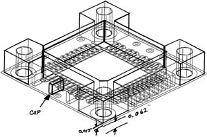
Controlled impedance socket
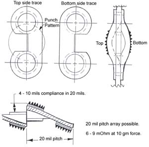
44 pin controlled impedance Particle Interconnect PLCC socket or interposer with singulate leads. Decoupling capacitors are within 0.100" of PLCC pad.
 |
 |
| Printed circuit board layout | Mechanical hold down |
Circuit layout for controlled impedance socket
D.U.T. board layout use for TDR measurement. The traces are narrowed to compensate for Z0 change due to devices present in the socket.
 |
 |
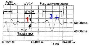
TDR of controlled impedance Particle Interconnect socket (interposer) on load board
 |
 |
||||||||||||||||||||||||||||||
|
|
||||||||||||||||||||||||||||||
|
|||||||||||||||||||||||||||||||
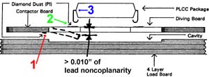
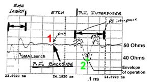
- Cursor at contact point on diamond dust/diving board with no part in socket.
- Trigger is continuously running at 10.0 kHz with step on.
- Demonstrated controlled impedance connector from contactor board to mother board using Particle Interconnect with impedance tolerance of 50 Ω ± 1 Ω.
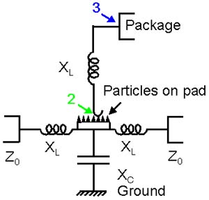
- Controlled impedance of J-lead going to package.
- Compensation (Point 2 on graph) to neutralize internal inductance and capacitance of PLCC package (Point 3 on graph).
- Particle Interconnect is 10 times better than SMA connector (Point 1 on graph).
- Additional work by MMS, TI, and HP.
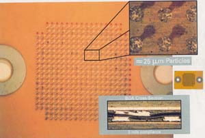
Particle Interconnect contact resistance vs. contact force
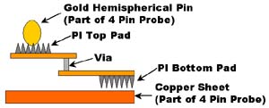
Gold probe to top side Particle Interconnect
Particle Interconnect's very low resistance results in higher current capacity.
- 1 mm pitch BGA interposer.
- 9.2 grams contact force (.0902 N, .020 lbs, or .325 Oz.)
- Contact resistance = .00433 Ω
 |
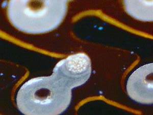 |
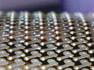
| Particle Interconnect array top side | Particle Interconnect bottom side close up |
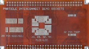
Examples
Demo sockets
One lead in each socket is deliberately removed, in order to prevent its use as an actual production socket.
 |
 |
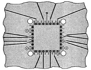
| 28 pin SOIC/SOJ; 20, 28, 32, 44 PLCC/LCC; 32 pin TSOP. |
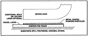
Particle Interconnect contact detail. |
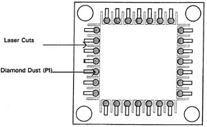
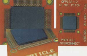
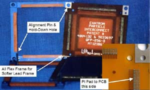
Particle Interconnect lead frame package
 |
 |
| Solder bumped chip (ILB) on Particle Interconnect lead frame (OLB). | Particle Interconnect bumped chip (ILB) on Particle Interconnect lead frame (OLB). |
Particle Interconnect Package (PIP)
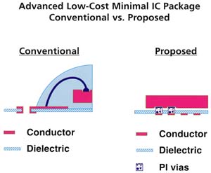
Advanced low-cost minimal IC package.
 |
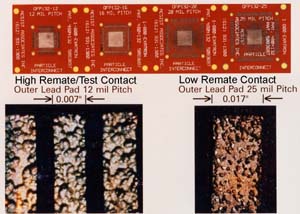 |
| QFP 132 lead, 0.012" pitch OLB (Outer Lead Bond). | Leadframe / Chip-On-Board socket & carrier. |
|
 |
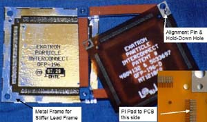
Alternative Particle Interconnect lead frame with holddown
Removable single unit - proof of concept.
 |
 |
| 0.025" pitch, 196 lead, ceramic QFP. | 0.020" pitch, 256 lead, ceramic QFP. |
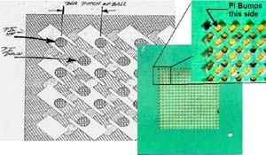
Particle Interconnect surface mount BGA socket
0.030" pitch, 19x19 version.
Particle Interconnect seasaw BGA socket
BeCu spring material with Particle Interconnect bumps on opposite sides of opposite ends of beam.
Particle Interconnect through-hole BGA socket
0.050" pitch, 15x15 version.
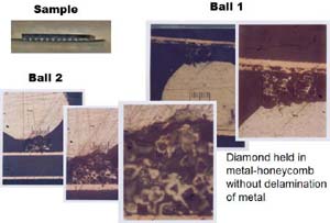
Particle Interconnect piercing SDRAM DDR1 package balls
- Demonstrating damage free performance when exposed to excessive loading.
- 60 pounds of force on 60 balls.
- Note minor depth of penetration.
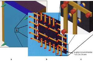
Particle Interconnect - MMS - TI - HP bare die probe
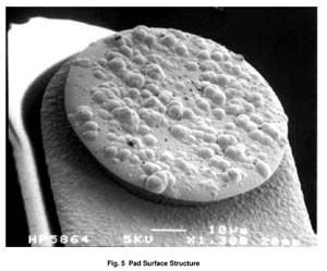
Proof of removable Known-Good-Die. Note single layer of particle on pad.
IEEE Transactions on Components, Packaging, And Manufacturing Technology
A Bare-Chip Probe for High I/O, High Speed Testing
Alan Barber, Keunmyung Lee, and Hannsjorg Obermaier
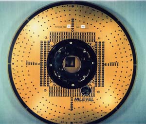
Particle Interconnect - Hughes Aircraft 1988 joint venture
Burned-in at 125 ° C for 168 hours.
 |
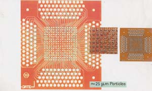
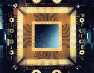 |
| 15 mil pitch, 188 lead, JEDEC Standard TAB test socket with 50 MHz high level D.U.T. tester. | 15 mil pitch, 188 lead, JEDEC Standard TAB test socket. |
Particle Interconnect - Hughes Aircraft 1988 joint venture in Known-Good-Die
Resulting in a supercomputer assembled with Known-Good-Die in 2" x 4" x .1".
Science/Scope 1989 Hughes Aircraft Company:
"A new technique for packaging large-scale integrated circuit (IC) chips will permit much denser packaging on the substrate than previously possible. High-density multichip interconnect (HDMI) technology, being developed by Hughes, is designed to meet the needs of the next generation of VHSIC II hybrid circuits, which require dense packaging with no signal degradation at frequencies over 100 MHz. HDMI packaging achieves these results using a multi-layer substrate, a polymer dielectric highly suited to fine line metallization processing, and lithography techniques capable of producing 10-micron line widths. The technology is expected to be used in radar, sensing, tracking and guidance programs."
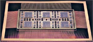
"The Data Memory Structure (DMS) multichip module is a very high speed cache memory system, switchable at high speed, to either of 3 input or output ports."
"HDMI can accommodate six 129K gate arrays (.640x.640 mil/die, 550+ pads/die; total 750,000 gates and 3,300 pads), 52 capacitors, and 24 - 15 nsec SRAM (32+ pads/die; total 750+), interconnected (using 70+ mil wire bond alleys) on a 2" x 4" = 8 in2 substrate having 368 I/O's."
"Performance of high speed circuits is also enhanced with low K polyimide dielectric used in the HDMI multilayer thin film (solder sealed ceramic leaded package) structure."
(All components tested/burned-in/speed sorted using PI resulting in 15+% yield improvement over production parts. Die price set at $5,000@ x 6 = $30,000, therefore DMS price >$100,000@)
PI's proposed removable die MCM-L/D/C to Hughes Aircraft.
Proposed to purchased a wafer for a total of $1,000 which was comprised of 300 die (5K gates/die .275 x .275 in.2/die, 180 pads/die for a total of 1,500,000 gates and 54,000 pads) interconnected on a 4" x 6" = 24 in.2 substrate. 50 mil pitch array yielded up to 9,600 I/O's.
Cost is further reduced by common low K polyimide multilayer PCB using 6+ mil pitch traces.
Environmental sealing of each die would also produce better reliability and upgradeability.
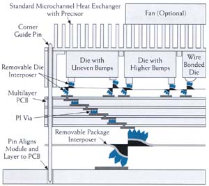
Removable die MCM
Removable die Multichip Module - L/D/C
|
|
 |
 |
| Removable die MCM | Louver contact |
- Low-cost heat exchanger designed for modular dissipation needs.
- Removable die locator (precisor) aligns all die on 0.010" edge-to-edge mosaic tile pattern of silicon.
- Precisor is accurately aligned by corner guide pins in heat sink.
- Removable die PI interposer sockets die to PCB and spring loads die against heat sink.
- Interposer is accurately aligned by corner guide pins in heat sink.
- Removable die PI interposers with 0.001" - 0.008" travel on 0.001" - 0.030" pitch are available.
- Removable multilayer PCB interconnects all die together with controlled impedance from die pad to die to pad.
- PI vias between laminate layers allow 0.002" "blind" vias by punching through adhesive layer during lamination.
- PCB is accurately aligned by corner guide pins in heat sink.
- Removable package PI interposer sockets package to PCB and spring loads package to PCB.
- MCM is accurately aligned and held to PCB by corner guide pins for manual or automatic insertion.
- Package interposers with 0.08"-0.020" travel on 0.010"-0.050" pitch with either peripheral or array patterns available.
- Die are removable by simply unstacking layers.
- Both bumped and wire bond die pads are mixable.