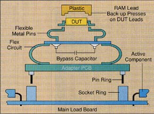
Test Socket
Particle Interconnect advantage
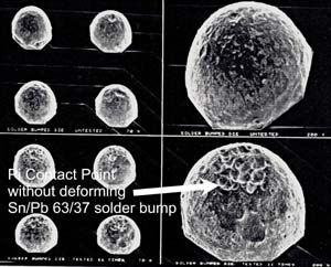
Diamond Particle Interconnect interposer vs. solder ball
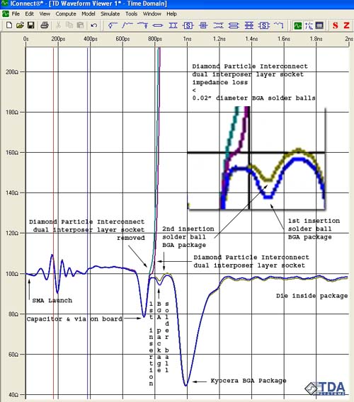
TDR data illustrates zero reactance and consistency of Diamond Particle Interconnect socket compared to soldered connection and SMA connector.
Particle Interconnect advantages
| Industry problem | Particle Interconnect solution |
| Traditional sockets are made up of springs or pogo pins to achieve compliance. However, at Gigabit speeds they create a large impedance discontinuity at the solder ball due to skin effect loss and impedance mismatch, degrading the system interconnect return loss. Therefore, a device can fail a functional test in a traditional socket even though it can pass the test when soldered to a board. | Particle Interconnect is presently used in the electronics testing industry for creating very high frequency sockets. The Particle Interconnect socket has exceptional long life (+1,500,000 remates) and very high reliability. Particle Interconnect creates a non-wiping remateable electrical interconnect on any electrical surface with the application of low mechanical force. This property allows a Particle Interconnect coated printed circuit board to be transformed into a remateable socket. |
| Pogo pin's large travel does not detect miss-sized balls on BGA packages. This result in package failure when soldered to PCB. | Particle Interconnect design allows one to tailor socket compliance to detect mis-sized BGA balls without signal speed reduction. |
| Currently BGA balls are replaced individually (www.finetechusa.com). | PI's solution is a single 2" stroke across 600 grit sand paper to planarize the balls by reducing the solder volume and then reshaping the solder balls by reflowing. |
| Industry data indicates that a considerable number of good devices are rejected and/or damaged by the repeated re-mating in conventional spring based sockets which need wiping action to make a good electrical contact. | The Particle Interconnect based socket use has improved overall yields in this type of application, by eliminating miss-contacts and lead damage to the device under test. |
| Companies developing and supplying high frequency integrated circuits face difficult challenges in attempting to characterize and emulate the packaged devices. | This problem can be solved by eliminating the test socket which normally sits on top of the DUT board and incorporating Particle Interconnect directly into the DUT board or by inserting a low profile Particle Interconnect based interposer between the device and the DUT board. |
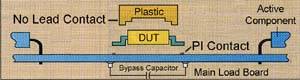
| A problem in high frequency testing and interconnects is the impedance mismatch between the device and related circuitry. This mismatch is typically caused by the use of conventional interconnect technologies with their long, uncontrolled impedance environment. Due to physical characteristics, conventional interconnects force long trace lengths between devices and related circuitry. All of these factors contribute to increased resistance (R), capacitance (C), and inductance (L). | The Particle Interconnect joint is a pressure only connection which requires no sliding or wiping action. The connection is a matched impedance connection, with no impedance mismatch, so there is no reflected energy, thereby reducing the amplitude of the reflected signal allowing for faster signal transmission with greater signal fidelity. |
| The wiping action required by conventional interconnect technology destroys and scars the metal surface that is being wiped. The wiping surface accumulates the wiped-off debris, and its non-conductive materials. With time, this accumulated debris prevents any electrical connection from being formed. | The absence of wiping action and the low force required to make connection combine to simplify the requirements of the mechanical hold-down. |
| Conventional contacts require 100 grams of contact force. At 100 grams per contact, the force level for a 227 point land grid array (LGA) package socket would be approximately 50 pounds. High compressive force of conventional connections require the inclusion of a backing plate to stiffen the receiving surface. | The Particle Interconnect equivalent 227 point LGA socket requires only 0.9 pound. Therefore, one can use adhesives, vacuum, and/or air pressure, besides low pressure springs and dips for providing hold-down forces. |
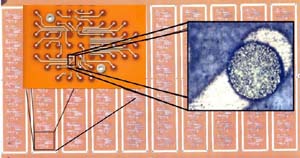
Test boards
Normally a standard bent-wire socket is used as contactor for automatic test equipment (ATE). The normal bent-wire contactor is limited to accept only one style package per contactor design. A high cost is incurred if many different pin count package/contactors must be stocked. Since handlers are longlife only a few contactors are required which results in a high cost per contactor due to tooling cost. |
A Particle Interconnect contactor consists of Particle Interconnect coated PCB or metal frame. This allows for flexibility in designing contactors with the shortest lead length possible. Also, multiple package styles can be nested in one design. The result is a significant cost savings and increased product throughput. The customer saves considerable time-to-market by using the fast response time of designing with Particle Interconnect, and avoids high tooling cost, or the purchase of many dedicated tester interface boards. Particle Interconnect interposer allows the device under test to be evaluated in the same configuration as when the device is soldered to the application board. This allows a 6 to 18 month time-to-market improvement because a more accurate characterization of the device. |
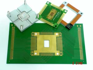
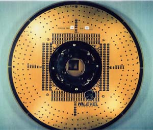
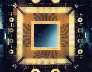
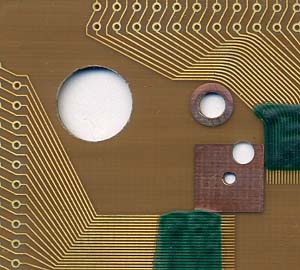
| Particle Interconnect Bare die test socket, and load board. |
|
Speed testing and binning for ICs
Increasing timing defects with small fabrication technologies require improving test quality. Therefore, at-speed testing is often necessary.
Particle Interconnect provides improved impedance uniformity and control at the tester to die interface. This allows accurate and reliable testing at higher clock frequencies and/or faster rise time, so that speed-binning can be reliably extended to higher performance.
Higher device yields are realized because smaller, more realistic guard-bands can be set, and testing can be performed at operating conditions.
Particle Interconnect can also be used as a reliable and cost effective means of test and burn-in of bare die and whole wafers.
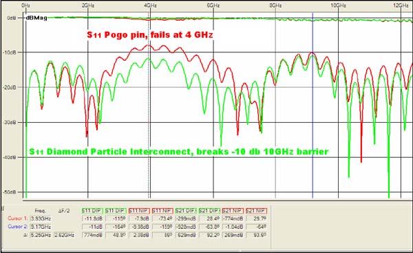
Particle Interconnect vs. pogo pin S11 parameters
The measured insertion and return loss shows a 4 GHz resonance at the solder ball causing PCI-X return loss failure below 6 GHZ. By replacing the standard pogo pin socket with Particle Interconnect socket the return and insertion was measured beyond 12 GHz, without modifying the board.
Lifetest comparison of Particle Interconnect vs. other sockets
Tested to failure.
This graph illustrates the exceptionally long remate life the Particle Interconnect coating provides a contact. Since the non-wiping action of the particles does very little damage to the mating surface, contacts last for 1,000,000 insertions or more. While this number is higher than the most applications require, it does testify to the robustness of connections using Particle Interconnect coatings.
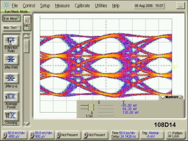
10 Gb/s PAM4 (Programmable Attribute Map) eye diagram
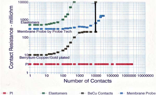
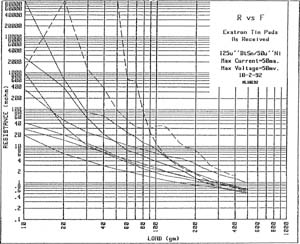
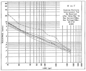
Particle Interconnect contact resistance vs. contact force
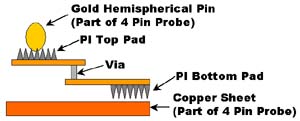
Gold probe to top side Particle Interconnect
Particle Interconnect's very low resistance results in higher current capacity.
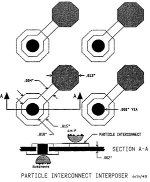
- 1 mm pitch BGA interposer.
- 9.2 grams contact force (.0902 N, .020 lbs, or .325 Oz.)
- Contact resistance = .00433 Ω
 |
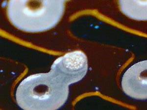 |
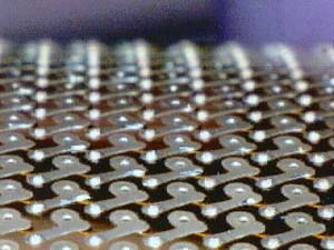
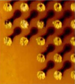
| Particle Interconnect array top side | Particle Interconnect bottom side close up |
Contact resistance (milli-Ohm) vs. holddown force (gram-force)
Courtesy of Amp
These graphs show how Particle Interconnect coated contacts compare to traditional scrubing contact surfaces as regard to contact force and resistance. They illustrate the exceptionally low contact force of Particle Interconnect, showing this force to be at the test limit of 10 grams.
More importantly, the graphs show how consistently Particle Interconnect coatings perform between remate cycles. While tin and gold plated contacts 40 to 100 gram range initially, this performance was inconsistent and tended to degrade between remates because of oxide growth.
0.25" diameter hemispherical probes vs. 63/37 tin-lead coated surface.
| Bright tin probe vs. control (no PI) | Bright tin probe vs. 20-25 μ PI |
 |
 |
|
. 0.010" BeCu, 0.250" Ni, 0.150" SnPb. . 20 to 80,000+ milli-Ohms, 1 to 9 remates. . No scrubbing action. |
. 0.010" BeCu, 0.250" Ni + PI, 0.150" SnPb. . 6 to 9 milli-Ohms (one ignored), 1 to 6 remates. . No scrubbing action against PI. |
| Gold Probe vs. Control (no PI) | Gold probe vs. 20-25 μ PI |
 |
 |
|
. 0.010" BeCu; 0.250" Ni; 0.150" SnPb. . 20 to 80,000+ milli-Ohms, 1 to 9 remates. . No scrubing action. |
. 0.010" BeCu; 0.250" Ni + PI; 0.150" SnPb. . 8 to 14 milli-Ohms, 1 to 8 remates. . No scrubbing action against PI. |
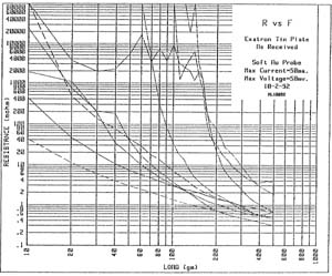
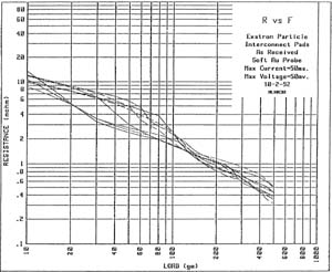
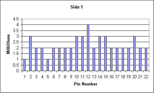
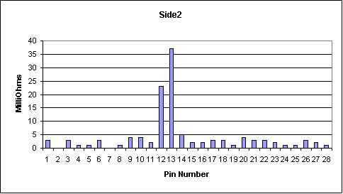
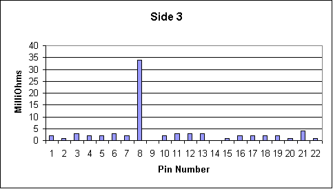
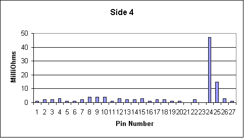
Test demonstrating reduced guard band
Plots of pin resistance deviation by pin number for 6 remates for each side of a QFP
Total variation for 6 insertions.
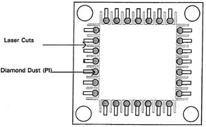
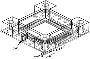
PLCC examples
Particle Interconnect PLCC universal test socket
Nesting multiple packages in one design.
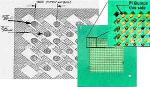
0.050" pitch, 20-84 lead with coplanar verification built-in.
|
|
BGA examples
Particle Interconnect socket replacing pogo pin
 |
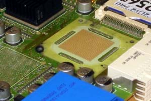 |
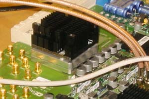
| Particle Interconnect socket with heat sink for 676 ball BGA | Particle Interconnect interposer for 676 ball BGA |
Particle Interconnect - Sandia Lab Known Good Die (KGD)
Known-Good-Die probe/burn-in. Proof of removable die MCM-L/D/C.
- 0.030" pitch 19x19 miniBGA.
- Burn-in at 125 ° C, 168 hours.
- 0 failures, 100+ runs, no deformation.
 |
 |
| 0 failures, 11 runs shown above. | Particle Interconnect surface mount BGA socket. |
 |
 |
| Particle Interconnect - Sandia mBGA interposer schematic. | Sandia mBGA interposer |
Particle Interconnect through-hole BGA socket
0.050" pitch, 15x15 version.
Particle Interconnect seasaw BGA socket
BeCu spring material with Particle Interconnect bumps on opposite sides of opposite ends of beam.
Tab examples
Particle Interconnect - Hughes Aircraft 1988 joint venture
Burned-in at 125 ° C for 168 hours.
 |
 |
| 15 mil pitch, 188 lead, JEDEC Standard TAB test socket with 50 MHz high level D.U.T. tester. | 15 mil pitch, 188 lead, JEDEC Standard TAB test socket. |
0.015" pitch OLB (Outer Lead Bond) - 0.006" pitch ILB (Inner Lead Bond) TAB (Tape Automated Bonding) tested/burned-in/speed-sorted.
- Excise line for flip chip mounting of TAB frame into finished MCM.
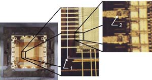
- Particle Interconnect ILB contact point onto 129k gate array.
Hughes TAB'ed test fixture
 |
 |
| Test fixture | Test fixture closeup |
Test fixture
Particle Interconnect MCM-L membrane test fixture
| Particle Interconnect used on flex-circuit material to form a translator bare-board test fixture. The translator is constructed by using a simple two-sided, plated-through-hole, printed circuit board (PCB), which is coated with Particle Interconnect on both-sides. The translator PCB accommodates the difference between off-grid test points of the unit under test (UUT) and the universal grid of the board test system. The bottom side matches up with the testers on-grid pads. Traces from the bottom side connect to the top side with plated-through holes. The translator PCB becomes the test fixture. |
0.010" pad, 0.015" pitch, 0.004" compliance. |
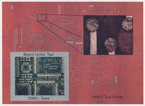
Particle Interconnect bare board membrane test fixture
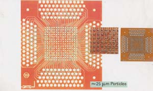
| The 0.020" pitch board (see insert) with more than 2400 test points and 2000 PCB has been tested with a single bareboard membrane test fixture. |
|
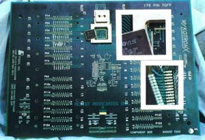
Particle Interconnect socket on load board
0.020" pitch 176 lead TQFP socket.
Controlled impedance to lead of package / die pad
Controlled impedance to lead of package
 |
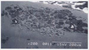 |
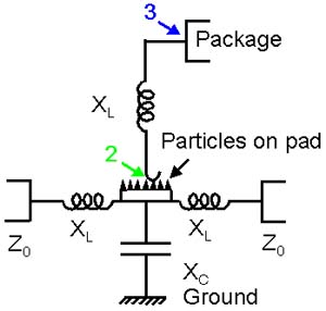
| Schematic for controlled impedance socket. | Surface of PLCC J-Lead after 30,000 insertions. Surface finish of lead passed steam aging test. |
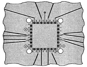
Controlled impedance socket
44 pin controlled impedance Particle Interconnect PLCC socket or interposer with singulate leads. Decoupling capacitors are within 0.100" of PLCC pad.
 |
 |
| Printed circuit board layout | Mechanical hold down |
Circuit layout for controlled impedance socket
D.U.T. board layout use for TDR measurement. The traces are narrowed to compensate for Z0 change due to devices present in the socket.
 |
 |
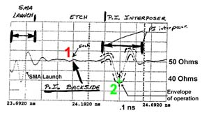
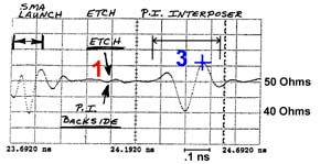
TDR of controlled impedance Particle Interconnect socket (interposer) on load board
 |
 |
||||||||||||||||||||||||||||||
|
|
||||||||||||||||||||||||||||||
|
|||||||||||||||||||||||||||||||
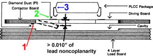
- Cursor at contact point on diamond dust/diving board with no part in socket.
- Trigger is continuously running at 10.0 kHz with step on.
- Demonstrated controlled impedance connector from contactor board to mother board using Particle Interconnect with impedance tolerance of 50 Ω ± 1 Ω.
- Controlled impedance of J-lead going to package.
- Compensation (Point 2 on graph) to neutralize internal inductance and capacitance of PLCC package (Point 3 on graph).
- Particle Interconnect is 10 times better than SMA connector (Point 1 on graph).
- Additional work by MMS, TI, and HP.