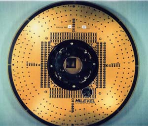
Burn-in Socket
- Particle Interconnect advantage
- Test results
- TDR Test Results
- Controlled impedance to lead of package / die pad
- BGA examples
- TAB example
- Removable die MCM
- SEM pictures of PI
Particle Interconnect advantage
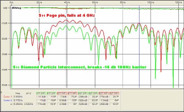
Particle Interconnect vs. pogo pin S11 parameters
The measured insertion and return loss shows a 4 GHz resonance at the solder ball causing PCI-X return loss failure below 6 GHZ. By replacing the standard pogo pin socket with Particle Interconnect socket the return and insertion was measured beyond 12 GHz, without modifying the board.
Test results
Lifetest comparison of Particle Interconnect vs. other sockets
Tested to failure.
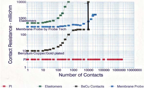
This graph illustrates the exceptionally long remate life the Particle Interconnect coating provides a contact. Since the non-wiping action of the particles does very little damage to the mating surface, contacts last for 1,000,000 insertions or more. While this number is higher than the most applications require, it does testify to the robustness of connections using Particle Interconnect coatings.
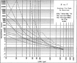
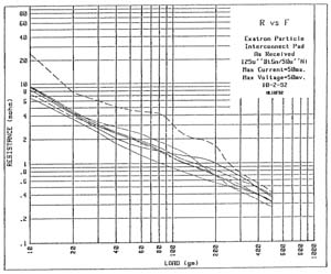
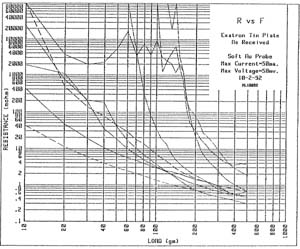
Particle Interconnect contact resistance vs. contact force
Gold probe to top side Particle Interconnect
Particle Interconnect's very low resistance results in higher current capacity.
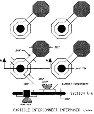
- 1 mm pitch BGA interposer.
- 9.2 grams contact force (.0902 N, .020 lbs, or .325 Oz.)
- Contact resistance = .00433 Ω
 |
 |
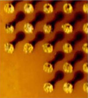
| Particle Interconnect array top side | Particle Interconnect bottom side close up |
Contact resistance (milli-Ohm) vs. holddown force (gram-force)
Courtesy of Amp
These graphs show how Particle Interconnect coated contacts compare to traditional scrubing contact surfaces as regard to contact force and resistance. They illustrate the exceptionally low contact force of Particle Interconnect, showing this force to be at the test limit of 10 grams.
More importantly, the graphs show how consistently Particle Interconnect coatings perform between remate cycles. While tin and gold plated contacts 40 to 100 gram range initially, this performance was inconsistent and tended to degrade between remates because of oxide growth.
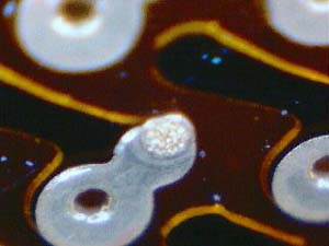
0.25" diameter hemispherical probes vs. 63/37 tin-lead coated surface.
| Bright tin probe vs. control (no PI) | Bright tin probe vs. 20-25 μ PI |
 |
 |
|
. 0.010" BeCu, 0.250" Ni, 0.150" SnPb. . 20 to 80,000+ milli-Ohms, 1 to 9 remates. . No scrubbing action. |
. 0.010" BeCu, 0.250" Ni + PI, 0.150" SnPb. . 6 to 9 milli-Ohms (one ignored), 1 to 6 remates. . No scrubbing action against PI. |
| Gold Probe vs. Control (no PI) | Gold probe vs. 20-25 μ PI |
 |
 |
|
. 0.010" BeCu; 0.250" Ni; 0.150" SnPb. . 20 to 80,000+ milli-Ohms, 1 to 9 remates. . No scrubing action. |
. 0.010" BeCu; 0.250" Ni + PI; 0.150" SnPb. . 8 to 14 milli-Ohms, 1 to 8 remates. . No scrubbing action against PI. |
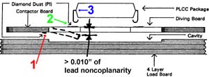
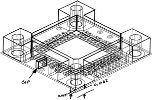
Controlled impedance to lead of package / die pad
Controlled impedance to lead of package
 |
 |
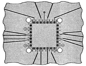
| Schematic for controlled impedance socket. | Surface of PLCC J-Lead after 30,000 insertions. Surface finish of lead passed steam aging test. |
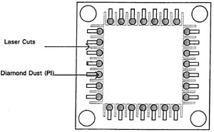
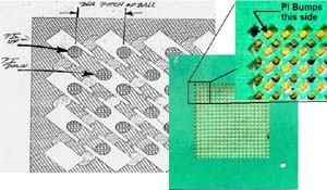
Controlled impedance socket
44 pin controlled impedance Particle Interconnect PLCC socket or interposer with singulate leads. Decoupling capacitors are within 0.100" of PLCC pad.
 |
 |
| Printed circuit board layout | Mechanical hold down |
Circuit layout for controlled impedance socket
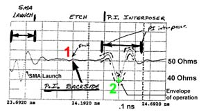
D.U.T. board layout use for TDR measurement. The traces are narrowed to compensate for Z0 change due to devices present in the socket.
 |
 |
TDR of controlled impedance Particle Interconnect socket (interposer) on load board
 |
 |
||||||||||||||||||||||||||||||
|
|
||||||||||||||||||||||||||||||
|
|||||||||||||||||||||||||||||||
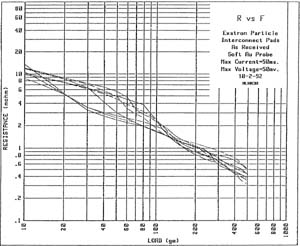
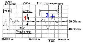
- Cursor at contact point on diamond dust/diving board with no part in socket.
- Trigger is continuously running at 10.0 kHz with step on.
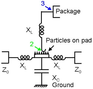
- Demonstrated controlled impedance connector from contactor board to mother board using Particle Interconnect with impedance tolerance of 50 Ω ± 1 Ω.
- Controlled impedance of J-lead going to package.
- Compensation (Point 2 on graph) to neutralize internal inductance and capacitance of PLCC package (Point 3 on graph).
- Particle Interconnect is 10 times better than SMA connector (Point 1 on graph).
- Additional work by MMS, TI, and HP.
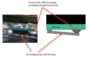
BGA examples
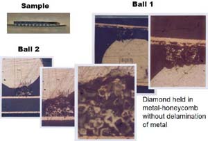
Particle Interconnect piercing SDRAM DDR1 package balls
- Demonstrating damage free performance when exposed to excessive loading.
- 60 pounds of force on 60 balls.
- Note minor depth of penetration.
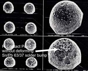
Particle Interconnect - Sandia Lab Known Good Die (KGD)
Known-Good-Die probe/burn-in. Proof of removable die MCM-L/D/C.
- 0.030" pitch 19x19 miniBGA.
- Burn-in at 125 ° C, 168 hours.
- 0 failures, 100+ runs, no deformation.
 |
 |
| 0 failures, 11 runs shown above. | Particle Interconnect surface mount BGA socket. |
 |
 |
| Particle Interconnect - Sandia mBGA interposer schematic. | Sandia mBGA interposer |
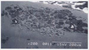
Beam bent against ball
Magnified 200X.
Particle Interconnect seasaw BGA socket
BeCu spring material with Particle Interconnect bumps on opposite sides of opposite ends of beam.
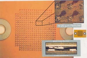
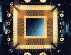
TAB example
Particle Interconnect - Hughes Aircraft 1988 joint venture
Burned-in at 125 ° C for 168 hours.
 |
 |
| 15 mil pitch, 188 lead, JEDEC Standard TAB test socket with 50 MHz high level D.U.T. tester. | 15 mil pitch, 188 lead, JEDEC Standard TAB test socket. |
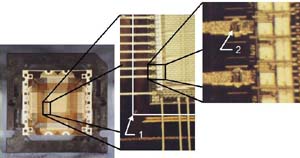
0.015" pitch OLB (Outer Lead Bond) - 0.006" pitch ILB (Inner Lead Bond) TAB (Tape Automated Bonding) tested/burned-in/speed-sorted.
- Excise line for flip chip mounting of TAB frame into finished MCM.
- Particle Interconnect ILB contact point onto 129k gate array.