MicroModules Systems (MMS)
Particle Interconnect Papers
- Particle Interconnect - MMS Spectrum MCM announcement
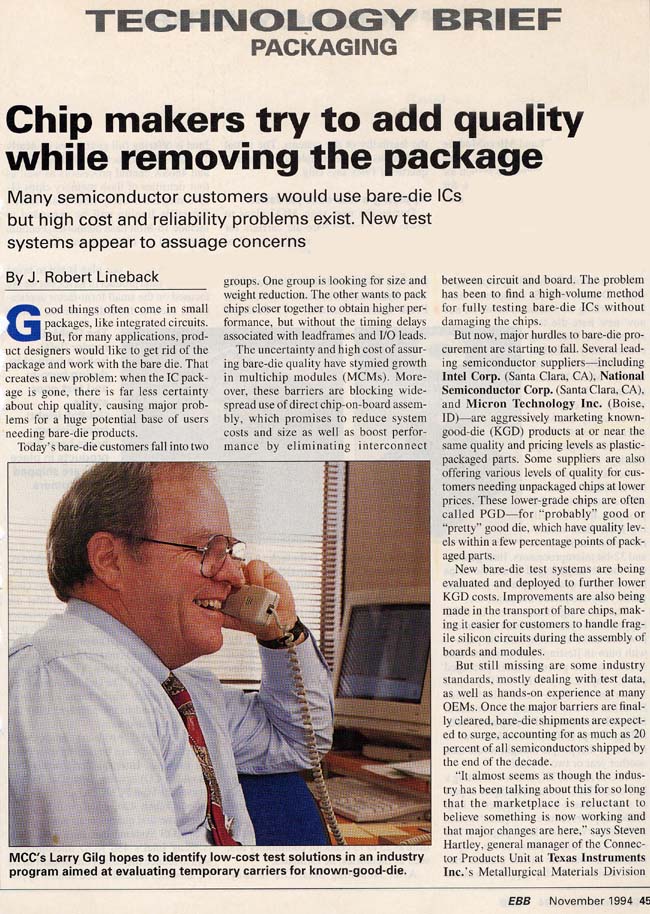
- Chip makers try to add quality while removing the package
- Particle Interconnect - MMS Known-Good-Die/Chip Scale Package
- Particle Interconnect - MMS reworking multichip modules
- Particle Interconnect - MMS - TI - HP bare die probe
- Particle Interconnect - MMS - Intel Known-Good-Die probe/burn-in
- Particle Interconnect - MMS - TI Known-Good-Die
Particle Interconnect - MMS Spectrum MCM announcement
For Dell laptop usage.
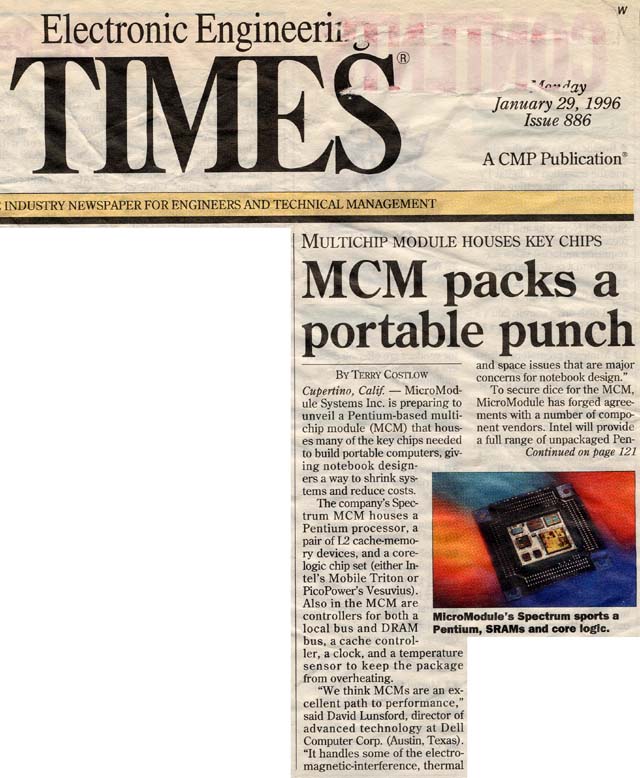
MCM Packs A Portable Punch
By Terry Costlow
January 29, 1996
Chip makers try to add quality while removing the package
By J. Robert Lineback
Electronic Business Buyer
November 1994
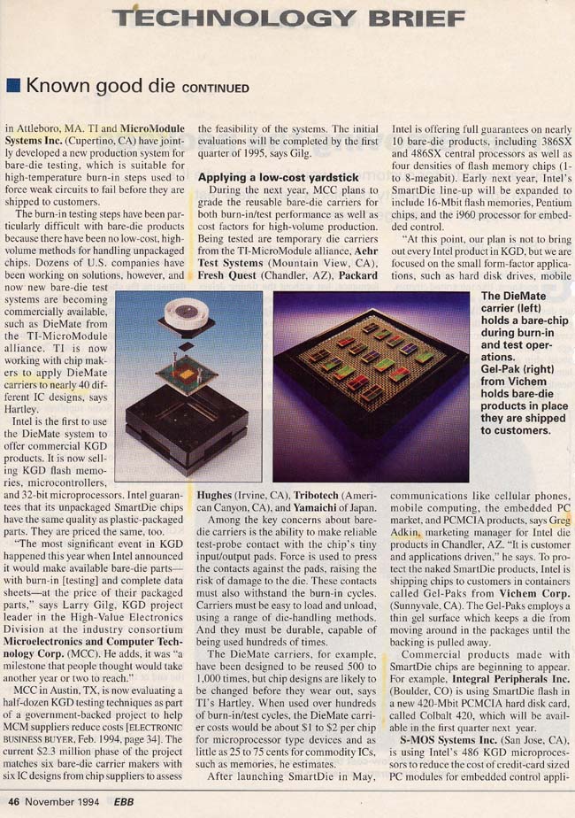
Particle Interconnect - MMS Known-Good-Die/Chip Scale Package
MCMs Getting The Goods
As The Technology To Deliver KGD Improves, Volumes Are Increasing
By Ann R. Thryft
September 12, 1994 A CMP Publication®
There's general agreement that multichip modules (MCMs) have the potential to reduce component space requirements dramatically, increase performance by 20% to 50%, and eventually cut costs. However, several obstacles remain before high-volume production is realized and unit costs become low enough to promote widespread acceptance of this promising technology.
Although MCM volumes are rising and prices have declined over the past year, many OEMs still consider the devices too expensive. A major portion of their cost - and the source of many headaches - relates to the acquisition of known good die (KGD) that have been fully tested. Compared with untested or inadequately tested unpackaged dice - which are readily available - KGD are difficult to obtain.
Another problem is that there are various definitions of KGD. Different suppliers are selling dice that have gone through varying levels of testing and have different levels of reliability. As a result, buyers may end up paying for unnecessary testing, or purchasing parts that have not gone through enough testing.
In addition, semiconductor suppliers find it difficult to transfer information about bare dice to MCM producers. But an emerging standard called the Die Information Exchange Format may help solve this problem (see sidebar, page 38).
Many consider KGD the enabling technology for MCMs. Die reliability is a big issue because it's extremely expensive to rework a failed MCM. "If you can't test the bare die, then you don't know if [the failed MCM] was a yield issue at the die level or at the module level," said Michael I. Grove, president and chief executive of MicroModule Systems (MMS), an MCM supplier in Cupertino, Calif.
Ideally, buyers want a bare die to have the same level of testing as a packaged part, but testing dice can be extremely expensive - and sometimes it's not even available. Furthermore, industry observers contend that full test and burn-in isn't always necessary to achieve the reliability of a packaged part.
Over the last year or two, semiconductor suppliers have started to see the KGD market as potentially lucrative, and have stepped up their interest in providing tested dice, said Stan Drobac, vice president of marketing for nChip Inc., a Milpitas, Calif.-based MCM supplier.
Several chip carrier systems - made up of a carrier, an insert that holds the die, and a socket - are now used by some larger suppliers. "Most people have focused in on some kind of [chip] carrier approach for testing and burning in die to produce KGD in the near term," Drobac said.
One such system is DieMate, which was developed by MMS and Texas Instruments Inc.'s Attleboro, Mass.-based Metallurgical Materials Division. The process is now used in volume by Intel Corp., and will be marketed to other semiconductor suppliers as well.
 The DieMate chip carrier system, developed by MicroModule Systems and Texas Instruments, includes (top to bottom) a lid assembly, a bare die, a thin-film substrate, and a test and-burn-in socket. |
 |
Bare dice on MCMs profoundly reduce space requirements, as demonstrated (left to right) by Intel Corp.'s 16-bit microcontroller (shown with a QFP), flash memory (with TSOP), 386 processor (with QFP featuring bumpers), and 486 processor (with QFP). |
According to Fariborz Agabdel, program manager at MMS, testing dice in a chip carrier can result in a savings compared with the testing of packaged parts. This is because some yield loss is typical with packaged parts, and different types of packages require different burn-in boards. The DieMate carrier holds one die at a time, but the carrier itself can be used over and over again.
This method may also be effective in testing dice before they are packaged, Agahdel said. "Once the volume of this method increases over the next two years - for certain applications where the yield isn't too great and the package is expensive - it will pay to use the carrier to test all dice before putting them into packages," he said.
Intel now offers several of its devices as KGD in the same volumes and at the same prices as packaged parts. The company began developing a KGD testing system about two years ago, according to Ron Williams, general manager of Intel's special products division in Chandler, Ariz. ''The goal from the beginning of our SmartDie program was to achieve price parity with packaged parts. Previously, prices for KGD have ranged from 1.3 times to three or four times the price of packaged parts."
Price parity has been achieved for most Intel devices, though. In fact, KGD generally cost the same as the least expensive packaged part, according to an Intel spokeswoman. The 33-MHz 386SX, for example, costs $18.40 in quantities of 1,000 for both the SmartDie and PQFP versions.
Intel's first step was to marry its sort and final-test programs in order to perform perform a full test at the probe stage while the dice are still in wafer form, Williams said. ''But since buyers also want burn-in, we partnered with TI and MMS to produce a chip carrier for die-level burn-in.''
"KGD can mean many different levels of test," said Greg Adkin, marketing manager for Intel's die products unit. "In our SmartDie program,we've taken it to mean the same level of testing we do on packaged parts." The dice operate over the full commercial temperature range of 0° C to 80° C, and full-speed AC-DC parametric testing is performed on them.
However, Intel won't offer all its products as SmartDie, Adkin said. "We're focused now on devices used in small-form-factor applications, such as portable computer and communications products." Intel presently sells high-density flash memory, microcontrollers, and microprocessors - including the Pentium - in SmartDie form. The industry has also speculated that Intel's next-generation P6 microprocessor will arrive as an MCM, but the spokeswoman would not comment on that.
Intel, along with contract manufacturers and packaging suppliers, has formed the Technical Alliance Program to help SmartDie buyers that have little experience with bare dice. Participants in the program include Anam/Amkor, Erso, Group Technologies, Jabil Circuit, MMS, SCI Systems, S-MOS Systems, Solectron, and Valtronic USA.
National Semiconductor Corp. uses a different carrier system developed by Fresh Quest. It also tests its KGD more thoroughly than it does its packaged parts, said James Kath, marketing manager for MCMs at the Santa Clara, Calif.-based company.
National offers four progressively rigorous levels of testing. Option 1 covers DC-probe testing only. "That's the standard [bare die] product [we sold] prior to KGD programs," Kath said. Option 2 adds lot-acceptance testing. Option 3 tests the die to AC and DC parameters at room temperature, and Option 4 adds burn-in.
National does not require full test and burn-in for all dice classified as KGD. Testing varies with the type of end-module, Kath said. For instance, Option 1 is used for mature, high-yield devices sold at the highest volumes for the simplest modules, while Option 2 testing applies to more complex modules, or to newer devices - such as the Ethernet controller. Options 3 and 4, on the other hand, test dice over the full military temperature range of -55° C to +125° C, and can be applied to dice going into high-reliability modules for space or medical products.
KGD tested to Option 1 specs cost the same or less than equivalent packaged parts this year, Kath said. The cost of dice tested to Options 2 or 3 is between 1.1 to 1.8 times the commercial price of packaged parts, and is close to parity on military devices. ''Currently, exact price parity can't be achieved on all four options because the volume hasn't been achieved yet,' Kath said. But by 1998, KGD tested to Option 3 should be close in price to commercial packaged parts, according to National's estimates.
National currently offers more than 70 standard logic products in KGD form at Option 3 or below. "We're working on four interface products and one linear device for Option 3 or below over the next few months," Kath said. Additional interface, analog, and memory devices will be added in the future. "We expect to add a minimum of 20 to 30 products per year to our KGD program," he said.
A third carrier system has been developed by Micron Semiconductor Inc. and an unidentified chip carrier supplier. "Some die manufacturers define KGD as dice that have received only functional and parametric tests at the wafer level," said Gene Cloud, vice president of marketing at Boise, Idaho-based Micron. "Other manufacturers' definitions include speed grading at elevated temperatures in addition to the functional and parametric testing."
Micron's definition encompasses both of these, plus burn-in. The supplier set out to develop a production system compatible with semiconductor fabrication equipment and test and assembly methods. The result is the KGDPlus process.
Many suppliers support the infrastructure of the MCM market. Cybex Technologies Corp., Richardson, Texas, has installed carrier loading and unloading systems at a number of semiconductor manufacturers, said president Robert Folaron. "We wanted to fill the void between a lab process and the volume manufacturing environment," he said. "Our automated loading and unloading equipment supports high-volume production of MCMs."
Cost remains the standard impediment. "Tooling charges ... are still too high in the industry for producing KGD in volume for the same price as packaged parts," said Ron Blankenhom, sales and marketing manager of San Jose, Calif.-based Nitto Denko America Inc., which has developed a chip carrier and insert system with Aehr Test Systems, Mountain View, Calif. Blankenhorn is confident that price parity will come soon, however.
While the majority of the industry uses wire-bond technology to attach dice to MCMs, there is one notable exception: IBM Microelectronics uses a solder ball flip-chip technology for its MCMs, most of which are used internally. It also uses an internally developed process for providing KGD that have been used internally. This week, however, IBM will introduce its first commercially available bare die in the form of a high-performance, 1-megabit static RAM, said Gary Hill, advisory engineer for KGD development at IBM in Essex Junction, Vt.
"Whether an application needs KGD depends on the number of chips, the amount of rework, the yield, and the complexity of die on the module" Hill said. While it may not be cost-effective to do full KGD testing on a module with only two dice, it is vital if a module has many chips because OEMs may need to determine which die has failed.
IBM is developing two wire-bond processes for testing KGD, and plans to have feasibility work completed by the fourth quarter with "qualified processes by the first quarter of 1995," Hill said. But IBM has no firm plans to provide wire-bonded die as KGD, according to Hill.
Motorola Inc.'s Semiconductor Products Sector has offered bare dice to select customers for some time. "[But] in terms of a wholesale offering of KGD to the marketplace, we have not done this, and it won't happen anytime soon," said Barbara Vasquez, director of technology for Motorola's assessment and development center in Tempe, Ariz.
For one thing, each product group in Motorola's semiconductor business operates independently. "Second, we're a vertically integrated company, and KGD primarily are used internally to build [Motorola] modules and systems," Vasquez said.
Several suppliers are looking ahead to the next step in KGD testing. "Longer-term solutions to KGD will be wafer-level burn-in," said nChip's Drobac. "It's inherently more economical." But reaching the next step could take two to seven years, observers noted.
Microelectronics and Computer Technology Corp. (MCC), Austin, Texas, has evaluated technologies that domestic suppliers are using to produce KGD for MCMs and application-specific electronic modules used in military systems.
MCC found that the cost of testing a KGD compared with testing a packaged chip can increase by up to a factor of two if the packaged product uses plastic rather than ceramic.
"Many die suppliers are targeting [cost] parity with plastic parts. However, in some cases parity with ceramic parts is adequate to justify investment in KGD," stated an MCC report published earlier this year.
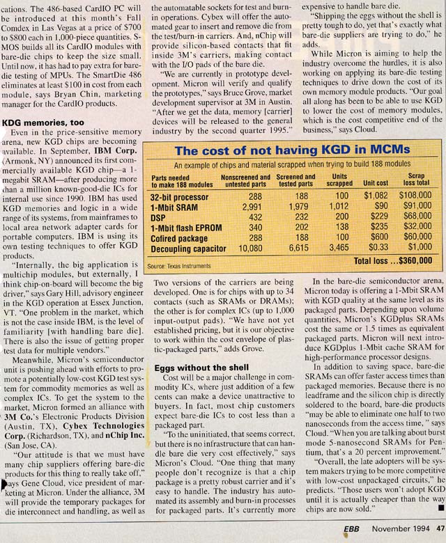
 The double-sided 2-Mbyte static RAM subsystem from National Semiconductor holds 16 1-Mbit SRAMs, six logic devices, and several decoupling capacitors.
DIE Format Aids KGD Availability
By Ann R. Thryft
One reason semiconductor suppliers have been reluctant to provide bare dice is the difficulty they find in transferring all necessary information to dice buyers, according to Stan Drobac, vice president of marketing for nChip Inc., Milpitas, Calif. "There is a lot of variation in that information, such as different CAD tools and formats," he said. Suppliers also aren't eager to provide proprietary information.
The Die Information Exchange Format proposes to solve those problems. "There are hooks in the DIE Format that allow the supplier to not provide sensitive data about the die," said Drobac. In most cases, only less sensitive proprietary data is needed, such as the location of bond pads on the die, and the dielectric material under the bond pad. The DIE Format lets semiconductor suppliers specify certain electrical characteristics of their dice without giving away propnetary circuit details, he added.
Version 1.0 of the DIE Format, released in April, provides administrative, material, geometric, electrical, thermal, supply, process, and logic simulation model data. It is both human-readable and electronic-design-automation-sensible, according to the DIE Industry Group, Beaverton, Ore. The group includes MCM suppliers, EDA vendors, semiconductor suppliers, and buyers. AT&T Microelectronics, Cadence Design Systems, Harris EDA, IBM, IDT Intel, Logic Devices, Mentor Graphics, Micro-Module Systems, Micron Semiconductor, Motorola, National Semiconductor, nChip, and Texas Instruments are members. Development of the DIE format and the formation of the DIE Industry Group were supported by funding from the government's Advanced Research Projects Agency.
| Ready For A Breakthrough | ||||
| North American MCM Revenue ($ Million) | ||||
| Market Segment | 1994 | 1995 | 1996 | 2000 |
| Data Processing | 671 | 1,206 | 1,838 | 10,166 |
| Communications | 301 | 384 | 505 | 1,569 |
| Industrial | 10 | 20 | 39 | 500 |
| Consumer | 3 | 5 | 8 | 65 |
| Military | 28 | 57 | 121 | 976 |
| Transportation | 1 | 4 | 6 | 80 |
| Total | 1,014 | 1,676 | 2,517 | 13,356 |
| Source: Dataquest Inc. | ||||
The new format provides timely, accurate information about the dice, and makes sure the information can be processed by the EDA tools used in the design process. Information can be created by a die supplier, released, and used to design an MCM in a few hours. Previously, MCM suppliers had to depend on data sheets, which take months to revise. However, the DIE Format streamlines the delivery of the latest information directly into EDA tools.
For the last year-and-a-half, the DIE Industry Group has worked to develop the spec as an industry standard, said Randolph E. Harr, senior scientist of the logic modeling group at Synopsis Inc., Mountain View, Calif. "We are going for ETA/ANSI standardization," he said, "and have contacted the International Electrotechnical Commission," a body that works with the ISO. The DIE Industry Group will become a formal working subcommittee of the Electronic Industries Association's electronic information group, and the DIE Format will be an official standard once it goes through the formal process. "We expect to initiate a formal ballot this fall, around October," Harr said. Final passage is expected by the end of the year.
Particle Interconnect - MMS reworking multichip modules
Attributes list shows reason for Particle Interconnect removable die MCM-L/D/C.
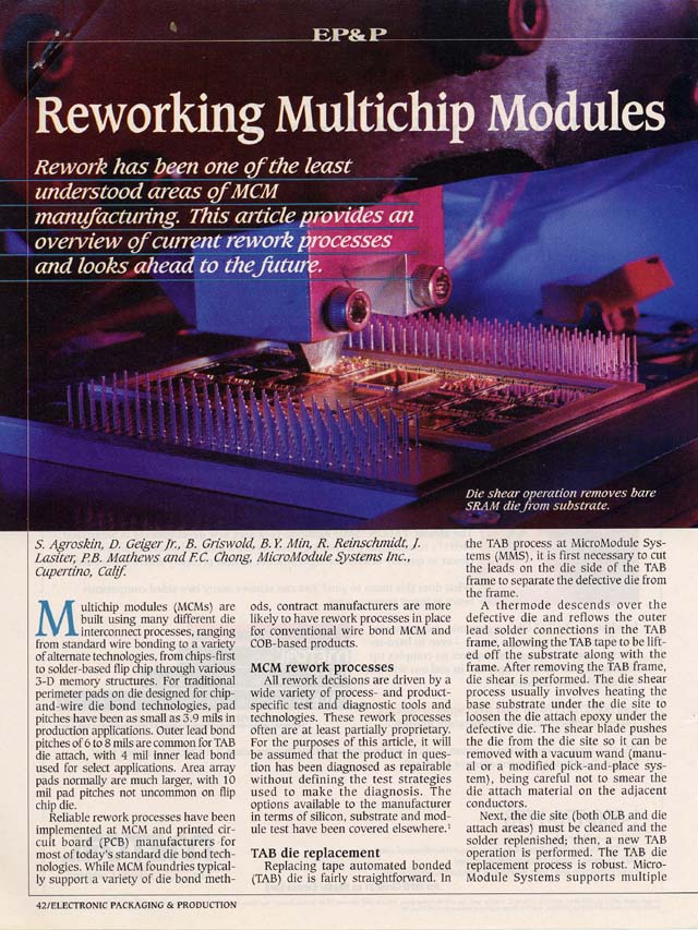
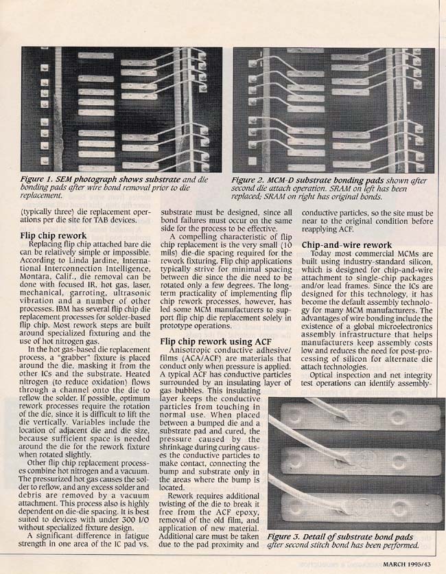
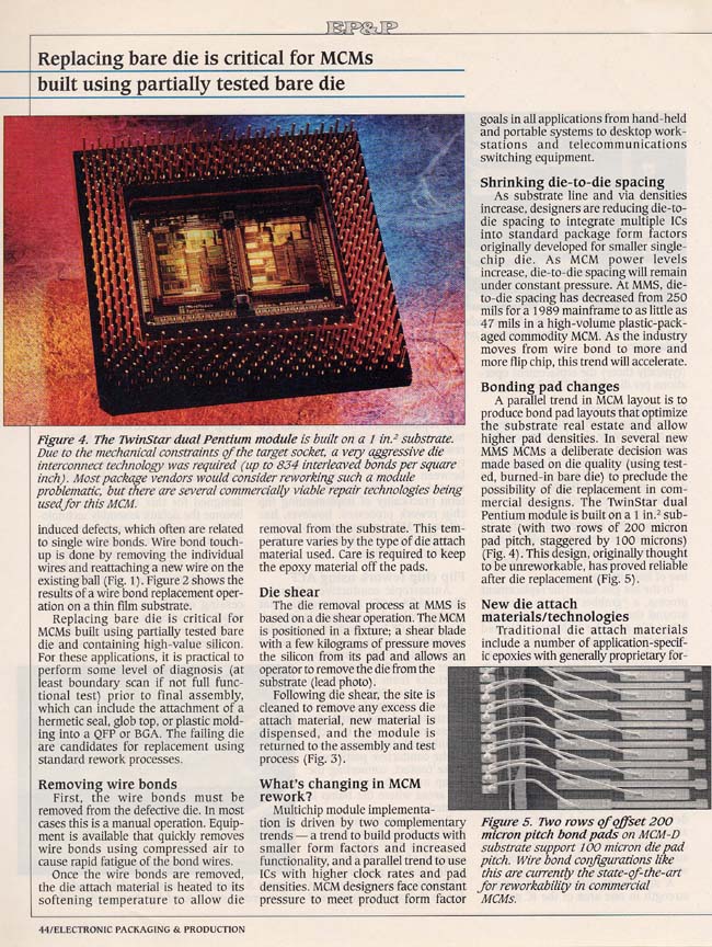
Reworking Multichip Modules
S. Agroskin, D. Geiger Jr., B. Griswold, B.Y. Min, R. Reinschmidt, J. Laister, P.B. Mathews and F.C. Chong
MicroModules Systems Inc.
Electronic Packaging & Production
March 1995

Particle Interconnect - MMS - TI - HP bare die probe
Proof of removable Known-Good-Die. Note single layer of particle on pad.
A Bare-Chip Probe for High I/O, High Speed Testing
Alan Barber, Keunmyung Lee, and Hannsjorg Obermaier
March, 1994
IEEE Transactions on Components, Packaging, And Manufacturing Technology
Abstract - We will describe a bare chip probing fixture for temporary interconnection of a VLSI tester to a die. It is capable of connecting to an area array of die pads, can operate beyond 1 GHz, and is extensible to 1000 signal I/O's. This probe has been adapted to an existing VLSI tester by attaching it to a custom DUT board and has been used to test operational silicon.
The fixture consists of a four metal layer membrane probe which is an enhancement to a previously described burn-in fixture with a novel alignment scheme and no-wipe contacting buttons. The probe is electrically connected to the DUT pcb with an array of button connections, and board I/O is through coaxial cables to the tester. A mechanical structure provides alignment of the pcb, button connector, and membrane probe while providing controlled pressure between the membrane and die, and at the same time cooling the die.
We will describe the electrical performance of the interconnect and the results of testing a circuit toggling at up to 1 GHz, compare them with another probing solution and describe future improvements contemplated. In addition, we will briefly describe the potential for use as a very fast bare chip burn-in fixture.
1 Background
The search for high performance, low cost computing has led many to consider mounting multiple large dice in multichip modules (MCM's). The penalty for mounting bad chips in MCM's is high, and well documented [1]. VLSI testers capable of operation at very high speeds and high I/O counts are available, but when the device under test is unpackaged, available probing solutions cannot match the performance of the tester. We sought a probing technology to match the bandwidth and accuracy of today's best VLSI testers [2].
The objectives of high bandwidth and accuracy led to these specific goals:
1. 1000 I/O's. Power and ground connections are additional for a total pad count of 1500-2000. Such a large number of device connections require an area array of pads. Solder bumped pads were tested, since that is probably the most common area array chip attachment method in use for VLSI today.
2. 660 Mbps.
3. Low distortion. When parametric measurements will be made at high speed, signal interconnections must have low loss, reflection, and crosstalk. And even more demanding, the power supplies and grounds must be able to supply many amps of current at very short rise times, with very little deviation in voltage. How much distortion is tolerable is dependant upon the application, of course, but here we will relate the distortion to the resulting degradation in tester accuracy specifications.
Potential wafer probing solutions were explored. The most aggressively designed cantilever probes still offer several nH of inductance and cannot accommodate the large I/O count and area pad array capability [3]. Arrays of spring loaded pins or buckling beams have been described that can meet the I/O count requirement [4, 5], but they have substantial inductance for the frequency or distortion requirement. The simulated performance of one such probe was examined and will be shown. Membrane probes or overlay fixtures have excellent high frequency properties, but the commercially available ones do not realize their full high frequency performance capability either because they do not have the multiple layer capability required to bring power and ground planes and microstrip connections to a chip area array or they are combined with sockets that have large uncontrolled impedances [6, 7, 8, 9].
We have built and tested a prototype bare chip probe system which meets the second and third goals, and has sufficient wiring density to meet the first. This design is a modification of a previously reported bare chip burn-in fixture [10]. The enhancements include additional layers to accommodate full microstriplines all the way to the chip area array pads as well as independent power and ground planes over the full area of the chip. Also the signal I/O design was modified for high frequency performance and the mechanical support structures were redesigned to accommodate a high speed VLSI tester.
2 Physical Configuration and Operation
 |
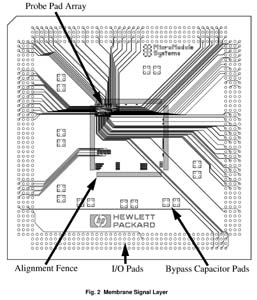 |
Figure 1 shows a cross section of the chip to probe interconnection. The probe itself is a four metal layer polyimide membrane supported by an aluminum frame. The membrane holds bypass capacitors and an integrated alignment fence which holds the die on the membrane. In this case, the chip has an area array of pads at 250 mm pitch with solder bumps applied. The chip and membrane are compressed between a lower support and an upper piston designed to apply a controlled force between membrane probe pads and chip pads. The four metal layers of the membrane include the probe pad layer with the oxide penetration features, one signal layer, one power distribution plane, and one ground plane. For our prototype, a membrane was designed to accommodate an existing test chip containing a variety of high speed receivers, data latches, drivers, and other test circuitry. Figure 2 shows a plan view of the signal layer. The alignment fence can be seen. Of the 122 chip signal I/O's, 114 are clustered in one corner of the chip, occupying about 5% of the chip area. With an additional signal layer this probe could accommodate 1000 I/O's. Chip I/O's are routed with embedded microstrip lines to pads over the aluminum support frame on the periphery of the membrane.
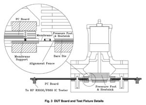
Figure 3 shows the assembled probe with the mechanical support and cooling structure. The connection between the membrane I/O pads and the DUT board is through an array of button contacts. These are crumpled gold plated molybdenum wire formed into a cylindrical shape and stuffed into holes in a thin polyetherimide interposer. Above the interposer is a spring alignment plate that centers the membrane over the interposer. The button contacts are compressed between membrane I/O pads and DUT board I/O pads. The interposer is aligned to the DUT board with four pins in slots that are designed to minimize misalignment during thermal excursions by maintaining a true center reference between board and membrane. Within the DUT board, striplines connect the button contact pads to SMA coaxial connectors. In operation, the membrane, holding the chip, is pretensioned from the bottom by a pressure plate. The membrane, interposer, and DUT board are all clamped between this bottom pressure plate and the upper support structure shown in Figure 3. The upper structure holds a pneumatically actuated pressure foot which applies controlled force against the chip. The pressure foot also serves as a heat sink and the upper support structure contains an air duct through which heated or chilled air can be forced to control chip temperature. The die under test is removed and replaced by raising the pressure foot, swinging the upper support assembly aside and moving the chip with a vacuum pickup. The whole DUT board assembly mounts into the DUT interface frame of the VLSI tester mainframe and coaxial cables connect the SMA connectors to the pin electronics within the mainframe. Alternately, either a pulse generator and oscilloscope, or a microwave vector network analyzer can be connected directly to the SMA connectors for system characterization or actual chip testing.
3 Making Reliable Contact
When probing large, dense arrays of I/O pads on a die there are several important requirements for making reliable electrical contact:
1. Alignment of probe and die pads in X and Y.
2. Compliance between probe and die pads in Z.
3. Penetration of non-conducting surface films.
4. Repeatability within a range of expected operating conditions.
In the prototype test fixture single dice are placed manually with a vacuum pencil into the integrated alignment fence. The fence opening is typically oversized by 0.024 mm to allow for the small variations in die size. The required dicing accuracy for this alignment scheme of ± .012 mm in overall size and pad-to-edge dimensions is well within the capability of today's dicing equipment.
A pressure foot gimbal and an elastically suspended membrane support assure probeto- die coplanarity. Plastic deformation of the solder bump compensates for most variations in bump height. Elasticity and flexing of the membrane allows probing of aluminum pads. Probably the most difficult task in making reliable contacts on conventional aluminum die pads is the penetration of the hard, non-conductive oxide film. Conventional tungsten wire probes on aluminum pads rely on a controlled wipe to break through. Spring loaded pin probes (pogo pins or needles) typically rely on stress concentration to displace oxides by cold flowing underlying metals. Oxide films on softer metals such as tin/lead used for solder bumps on flip-chips are generally easier to break and require a relative small amount of force to displace. Buckling beam probes used on solder bumps are normally designed to have a small wipe as well as sufficient force to displace oxides. In all cases probing must not contaminate or destroy the die pad or solder bumps so that subsequent processes can be performed successfully. Wire probe marks on aluminum pads, for example, could interfere with the solder bump processes.
Wear and contamination of probe tips or pads is an issue for long term reliability. Buckling beam probe users have reported a build-up of tin/lead and its oxides on probes used for solder bumps. A cleaning procedure at regular intervals is required for reliability. Only a relative small number of mating cycles with the membrane probe were tested at this time; more extensive tests to demonstrate reliability are under way.
Figure 4 shows the membrane probe pads employed in this test. They rely on stress concentration produced by a unique surface structure (Figure 5) to achieve redundant contacts on each pad or solder bump. Previous tests of burn-in sockets using identical pad structures on a membrane and contacting aluminum pads on a die indicated predictable contact resistance over a number of mating cycles and temperature ranges [10]. Our tests were focussed on demonstrating feasibility of the described technology for a test and burn-in application of solder bumped flip chips. Figure 6 shows the result of early probe tests. Stable contact resistance is reached typically at about 10 gram/bump with solder bumps and 20 gram/pad with aluminum pads. A force greater than 20 gram/pad results in severe deformation of the solder bumps requiring an additional reflow step prior to assembly. More extensive tests to validate probing of large arrays are under way using test chips with a number of daisy chains and four wire test pads.
4 Electrical Performance
 |
 |
The probe was measured with a microwave vector network analyzer, tested with a high speed pulse generator, and operated installed in a VLSI tester. An electrical model was built and compared to the measured data in the frequency domain. That electrical model was then used in the time domain to explore the effects of the probe on timing measurements made on a high speed CMOS circuit. Finally, these effects were compared to those predicted for another high performance probe using buckling beams.
Figure 7 shows the round trip frequency response from the connector on the DUT board through the pc board, through a membrane line, through a very short line on the chip, and back out through a similar path to another DUT board connector. This is the magnitude of the S21 scattering parameter as measured with a 50 W microwave network analyzer. Also shown is the frequency response as modeled with microwave design software. Figure 8 shows the model used to simulate the network with commercial analysis software. The coaxial connectors, PCB traces, and membrane probe traces are described by their physical dimensions and static electrical characteristics (i.e. dielectric constant and conductivity). The capacitance of the button connector pads and chip I/O pads are the calculated parallel plate capacitances. The inductance and resistance of the probe contacts themselves were calculated in a way described below. Good agreement is seen between measured and modeled responses.
In addition, crosstalk between adjacent lines was measured as follows. 50 W microwave probes [11] were used to contact two adjacent active pads of the membrane probe. Each active pad has an adjacent ground pad and is connected via the line on the membrane to a button contact at its periphery. In this measurement the probe was not mounted in the DUT board so the button contacts were unterminated. The microwave probes, in turn, were connected to the microwave network analyzer with coaxial cables and the analyzer was calibrated at the microwave probe tips, thus establishing a reference plane at the membrane probe contact point. An S21 measurement with this arrangement yields the crosstalk between adjacent lines and includes the effect of coupling between the probe tips, the lines on the membrane, and the button connectors. It also combines forward and backward crosstalk components since backward crosstalk is measured directly and forward crosstalk is reflected from the unterminated button connector and measured. The crosstalk was measured in the frequency domain and converted to time domain to give the peak voltage induced. For 200 psec risetime edges the p-p crosstalk was under 0.5% and for 75 psec risetimes it was approximately 2%. The value is low because the membrane lines are close together for only a very short distance near the chip pads.
 |
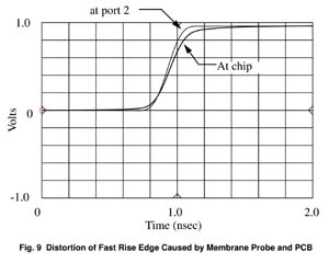 |
The signal distortion contributed by the membrane line and probe tip was simulated through use of the model of Figure 8. Reference [12] contains a good discussion of the signal distortion of fast edges caused by lossy lines such as this. The lower (and longer) path from port 2 to the chip interface was simulated and the frequency domain data converted by Fourier transform to the time domain to examine the response to a unit step input at port 2. The result is shown in Figure 9 with the bandwidth limited to produce a 200 psec step rise time. The input step has been translated in time to coincide with the output step and adjusted by 5% in scale to match the d.c. levels of the input step to allow a direct comparison of input and output edge shapes, as described in [12]. The transition from fast-rise region to slow-rise region caused by line resistance is seen to occur very high on the waveform, contributing little to waveform distortion and delay in the middle portion of the rise. This transition will occur at:
Vtt / Vot = e(-Rl)/(2Ro)
where R is the line resistance per unit length, l is line length, and Ro is the real part of the line characteristic impedance. In this case, 93% of the resistance is in the membrane portion of the line (R=2.3 Ω/cm, l=1.874 cm), the rest in the PCB portion (R=28.5 mΩ/cm, l=10.55 cm). Combining these values into the above expression yields a transition point at 95% of the output step. Keeping this transition point high on the waveform reduces its impact on the device being tested, whose switching point will typically be near the midpoint of the waveform.
 |
 |
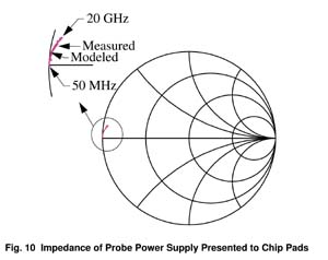
Perhaps more difficult and important than a good quality signal path is a good quality power and ground connection to the DUT. The ideal power supply would deliver amps of current at very fast rise times with no voltage deviation at the chip connections. This requires that a source of charge be available to the chip terminals with very little inductive reactance, a burden which falls heavily on probe design. Another way to look at this requirement is to say that the impedance presented to the chip by the probe power supply terminals be very low at all frequencies. Failure to meet this requirement at high frequencies will cause power supply voltage to change when fast steps of current are required. Failure to meet it at low frequencies will cause power supply voltage to change when sustained surges are required. The high frequency requirement is typically met by placing bypass capacitors as close to the chip as possible. Any resonance or high impedance will result in a ringing or glitching power supply voltage with large numbers of simultaneously switching drivers on the chip. This membrane structure provides a nearly ideal implementation of this high frequency requirement by devoting a whole metal plane to power supply and another plane to ground and by providing large value bypass capacitors close to the chip. To evaluate the contribution of the probe to meeting this high frequency requirement a measurement of the impedance presented to the chip by the probe was made. This measurement was made directly at the probe pads by probing with the same microwave probes and network analyzer configuration described above. The probe was not installed in a DUT board. Figure 10 shows the result plotted on a Smith Chart. It certainly approaches the high frequency ideal of a short circuit from 50 MHz to 20 GHz. In addition, a simple lumped equivalent circuit, Figure 11, was generated and fitted to the measured response. This equivalent circuit was also used for the signal line to chip transition described above since this transition is identical for signal connections and power connections.
D.C. power supply performance may also suffer with a membrane probe due to the high resistance of the thin film metallization, only 2 mm thick with sheet resistance of about 10 mW per square. In this case, however, with a full plane devoted to power supply and ground each and with power delivered from all four sides of the membrane, there is only about 1/8 square, or about 1.25 mW of power supply and ground resistance.
 |
 |
 |
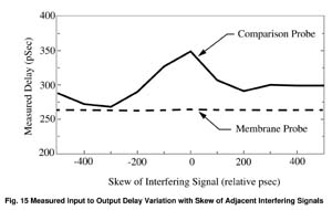 |
Each of the measurements and simulations above was carried out in a 50 W environment. We simulated performance in a measurement environment by using the signal and power supply models described above combined with models for a CMOS inverter and line driver as the device under test (DUT) in a SPICE simulation. The CMOS circuits used 0.6 mm gate length devices with a line driver capable of a 200 psec risetime into a 50 W transmission line. Three circuits were driven simultaneously in order to study the waveform and delay distortion created by interference from neighbor circuits. In addition, we created an electrical model for another high performance area array probe and substituted this model for the membrane probe model to compare the performance of the two. The three devices under test are contacted by a small array of ten probe points, three inputs, three outputs, and four power supplies. The power supply probe points were positioned between DUT's to reduce interference among them. Figure12 shows the arrangement for the comparison probe case. The model for this comparison probe was an array of ten mutually coupling inductors with inductance values computed from published dimensions [4]. The computed self inductance of a single probe was 4.5 nH and the mutual inductance varied from 2.9 nH for nearest neighbors to 1.58 nH for diagonally opposite neighbors. For the case of the membrane probe, the probe tip model of Figure 8 was substituted for each of the inductors in Figure 12. To study the effects of just the probe, a perfect power supply was assumed on the tester side of the probes. The SPICE connection to the probes (simulating the tester) was through 50 W transmission lines and the input signals were single 200 psec risetime edges simultaneously applied to all three circuits. Resulting waveforms for the center of the three circuits are shown in Figures 13a and 13b. Distortion of the step output waveform as well as power and ground voltage deviations are evident in the comparison probe. In many digital test applications these distortions are quite acceptable as long as data can be successfully toggled into and out of the DUT. However, if one wishes to make an ac parametric measurement, such as setup time, delay, or maximum frequency of operation, they can do damage. For example, if the edge timing of two devices is varied while examining the delay through a third device, the power supply noise caused by the two will be coupled into the third. This is illustrated in Figure 14. To the waveforms of Figure 13b have been added a set of waveforms,again for the center circuit,but in this case the two nearest neighbor signals are skewed 300 psec earlier. The power supply coupling has moved the output edge under observation by about 100 psec. Figure 15 shows how the measured delay through the center of the three DUT's in this example varies as the skew of the two adjacent edges is varied for both the membrane and the comparison probe. Such delay variations would be very difficult to calibrate out in a practical measurement situation and would contribute directly to measurement inaccuracy. In other words, this 100 psec delay variation adds directly to the tester's specifications for edge placement accuracy and resolution, which in some testers is at least 50 and 10 psec respectively.
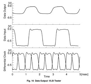
The probe was also evaluated with a test chip containing a variety of high speed bipolar receivers, latches, and drivers. Figure 16 shows output data after being latched into and out of the chip at 1 Gbps using a high speed data generator and oscilloscope.
5 Future Work
This first prototype has suggested to us additional analysis and product improvements that are now planned:
1. Reliability Testing. Tests with large numbers of mating cycles with solder bump metallization.
2. Lower loss lines. The loss in the coaxial cables can be reduced by using larger cables. The use of teflon dielectric in the DUT board results in lower loss lines and the membrane itself can be designed smaller, and the lines shorter, if an additional metal layer is used for signal distribution.
3. Eliminate button contacts. The existing pressure connection between the probe pads and solder chip metallization seems to be very workable. We believe we can extend this technique to the I/O pads and eliminate the whole button and interposer structure, making a direct pressure connection between the I/O pads and DUT board. This will simplify the structure and reduce the size of the largest reflection producer, the membrane pads.
4. Use for burn-in. A method has been developed [13] to screen for infant mortality reliability problems by making ac parametric and functional tests while rapidly ramping device temperature. It is more sensitive than traditional High Temperature Operating Life burn-in and can be done in about a minute on a high speed VLSI tester with proper chip handling and temperature control. This probing method would allow such screening to be done in the bare chip form, saving the cost of packaging devices which would ultimately fail HTOL burn-in.
6 Summary
We have described a bare chip probing technology that can contribute to solving the MCM Known Good Die problem. It is easily adaptable to a VLSI tester and allows chip testing with large numbers of high data rate signals with either peripheral or area array connections. The electrical properties allow highly accurate delivery of signals and power to the chip under test. Future developments include higher performance, simpler structure, and use simultaneously for test and burn in.
Acknowledgements
Thanks go to Chung Ho and Fariborz Agahdel of MicroModule Systems for the design and fabrication of the membrane, and to Steve Dielman and Matthias Werner of Hewlett Packard's Semiconductor Systems Center for training on and use of their HP83000 VLSI tester.
References
[1] D. A. Doane and P. D. Franzon, Multichip Module Technologies and Alternatives: The Basics, Chap. 13, Van Nostrand Reinhold, New York, 1993.
[2] H. Engelhart and U. Schottmer, "High Performance Pin Electronics with GaAs--A Contradiction in Terms", International Test Conference 1992 Proceedings, pp. 538- 545, 1992.
[3] E. Subramanian and R. Nelson, "Discover the New World of Test and Design", International Test Conference 1992 Proceedings, pp. 936-939, 1992
[4] D. J. Genin and M. M. Wurster, "Probing Considerations in C-4 Testing of IC Wafers", The International Journal of Microcircuits and Electronic Packaging, Volume 15, Number 4, pp. 229-238, Fourth Quarter 1992.
[5] S. Kasukabe, S. Harada, T. Maruyama, and R. Takagi, "Contact Properties of the Spring Probe for Probing on a Solder Bump" Proceedings of the Thirty-Eighth IEEE Holm Conference on Electrical Contacts, pp. 187-190.
[6] T. Fisher and J Kister, "Reducing Test Costs for High-Speed and High Pin-Count Devices", pp. 96-98, EE-Evaluation Engineering, February 1992.
[7] B. Leslie and F. Matta, "Membrane Probe Card Technology", International Test Conference 1988 Proceedings, pp. 601-607, 1988.
[8] R. Parker, "Bare Die Test", Proceedings of the 1992 IEEE Multi-Chip Module Conference", pp. 24-27, 1992.
[9] M. Andrews et al, "ARPA/WL ASEM Consortia for Known Good Die (KGD)", Microelectronics and Computer Technology Corporation, 1994.
[10] F. Agahdel, C. Ho, R. Roebuck, "Known Good Die: A Practical Solution", Proceedings of the 1993 International Conference and Exhibition on Multichip Modules, pp. 177-182, 1993.
[11] D. Carlton, K. Gleason, E. Strid, "Microwave Wafer Probing", Microwave Journal, vol. 26, pp. 747-748, 1990.
[12] M. Lin, A. Engvik, J. Loos, "Measurements of Transient Response on Lossy Microstrips with Small Dimensions", IEEE Transactions on Circuits and Systems, vol 37, number 11, pp. 1383-1393, November 1990.
[13] T. E. Figal, "Below a Minute Burn-in", United States Patent 5,030,905, July 9, 1991.
Particle Interconnect - MMS - Intel Known-Good-Die probe/burn-in
Proof of removable die MCM-L/D/C.
Next Generation Burn-In Development
David Gralian
IEEE Transactions on Components, Packaging, And Manufacturing Technology
Abstract - Die level burn-in (DLBI) and wafer level burn-in (WLBI) are two technologies that are being investigated to address the growing industry demand for product shipped as "known good die" (KGD). Commercial DLBI technology is now in the prototype evaluation and development stages. WLBI technology is now being seriously discussed in the industry and will require significant development effort. The major development area for the WLBI process will involve the technology to do whole wafer probing. Potential whole wafer probe technologies are being evaluated and there are four that look promising. Detailed cost analysis for DLBL and WLBI has been performed, using the current package level burn-in (PLBI) cost for comparison. DLBI is an evolution from PLBI and is a viable near-term solution (i.e., technology availability, cost) that will support the development of a KGD product line. WLBI appears to offer a long-term solution for supplying both KGD and packaged product, although the development path is revolutionary, and will entail more risk and years to fully develop.
Index Terms - Burn-In, known good die, KGD, die level burn-in, DLBI, wafer level burn-in, WLBI, multi-chip module, MCM, cost model.
Manuscript received August 20, 1993; revised December 30, 1993.
The author is with Intel Corporation, 5200 N. E. Elam Young Parkway. MIS AL4-61, Hillsboro, OR 97124-6497, USA.
IEEE Log Number 9401394.
I. INTRODUCTION
INTEL CORPORATION HAS BEEN evaluating future directions for semiconductor integrated circuit (IC) burn-in. Burn-in is the process of screening out process dependent latent defects from a product and thereby improving the product's outgoing quality and reliability. For Semiconductor components, burn-in is the process of subjecting the product to temperature and voltage stresses in excess of normal operating conditions for specific periods of time. This accelerates the product through the early part of its life cycle allowing removal of the products that would have failed during that time.
It is too early in the development phase to present much hard data due to availability and confidentiality. However, this paper presents some of the current thoughts, views and understanding from the evaluations on two new burn-in (BI) technologies being investigated and developed. They are die level burn-in (DLBI) and wafer level burn-in (WLBI). DLBI is the ability to handle, contact and do burn-in stress on a single IC die, while WLBI is the ability to contact every die location simultaneously on an entire wafer and perform the defined burn-in stress. The motivation for developing these new methods is the rapidly emerging need in the semiconductor and multi-chip module (MCM) industries for 'known good die' (KGD). In the industry, 'known good die generally refers to a non-packaged IC die that has been through the burn-in and test process similar to packaged IC product, making the die product equivalent in quality and reliability.
In developing a next generation burn-in method, it is very important that it be developed from a total production burn-in process perspective and not just as an engineering tool. With that in mind, the following basic rules are being used in selecting the best concepts, technologies and defining the new process.
- Meet all product quality and reliability screening requirements.
- Be cost competitive with the current production burn-in process for packaged product.
- Support long term strategic product directions (e.g., KGD sales, multi-die packages).
- Be technically feasible with acceptable risks (i.e., realistic).
- Be compatible with the existing IC component manufacturing flow.
Using these decision filters influences the direction of the next generation burn-in technology development, by providing basic boundary conditions that will help ensure the delivery of a production-worthy next generation burn-in process. These decision factors are used during the evaluation of both the DLBI and WLBI technologies described in this paper.
II. DIE LEVEL BURN-IN OVERVIEW
The technologies necessary to support die level burn-in are currently in development, with a number of suppliers announcing they are actively pursuing solutions to this market need. DLBI capability really started becoming commercially available in the 1993 timeframe and some leading semiconductor companies expect to have low volume DLBI & Test production in place during 1994 and high volume production in 1995.
As illustrated in Fig. 1. DLBI will be an extension of the existing Package Level Burn-in (PLBI) and will use most all of the existing Burn-in equipment and process. DLBI involves the development of a die carrier (basically a temporary package), that will fit into a socket on the burn-in board and will use the same burn-in ovens and burn-in board loader/unloader equipment. With this approach the only areas needing significant development will be the die carrier and the associated die handling capability. The die carrier will also be able to use the existing Component Test equipment with relatively minor changes. The final result is that DLBI will fit well into the existing IC manufacturing process for both the burn-in and test steps, which means quick implementation with controlled risk.

Fig. 1. Die level burn-in overview.
The most comprehensive evaluation of DLBI technologies has been done by the 'Consortia for KGD Program' at Microelectronics and Computer Technology Corporation (MCC) as part of a ARPA (Advanced Research Projects Agency) funded project [1]. This consortia, participated in by 37 different companies, developed a detailed list of 'Technology Assessment Guidelines' to score/rate each potential DLBI technology. Shown in Table I, with permission from MCC, is a chart taken from the detailed report, 'Consortia for KGD Phase I Report' (December, 1993), summarizing the results.
TABLE 1
MCC DLBI TECHNOLOGY ASSESSMENT
III. DIE LEVEL BURN-IN FLOW DIAGRAM
Shown in Fig. 2 is the basic product flow necessary to support the DLBI process. From a burn-in and test perspective, this adds complication and cost, versus a package product process, because it adds the die-to-carrier load & unload steps, adds the carrier clean step and requires some modifications to the existing bum-in board load/unloader equipment and the test handler equipment.
Fig. 2. Die level burn-in flow diagram.
For DLBI process development, the areas of primary concern will involve the handling and environmental integrity of the bare die to prevent damage to the die. For die handling issues, particular attention will be needed during the die to carrier load and unload steps and the carrier cleaning process. Die environmental integrity issues will involve ensuring that nothing in the carrier design and the burn-in and test steps will cause any degradation in the die's performance characteristics (e.g., reliability, electrical/speed characteristics, wire bonding, die attach).
IV. WAFER LEVEL BURN-IN OVERVIEW
Shown in Fig. 3 is a simple conceptual view of what a WLBI system might look like. Basically it's a series of individual automatic whole wafer probing stations supported by a central automated wafer distribution system. Each wafer probing station would consist of a whole wafer probe-head, a wafer alignment system, a thermally controlled x-y-z wafer stage. DUT Power Supplies, DUT signal driver electronics and station controller. There are other possible implementations, but this is the one we will use for this paper. This concept requires no additional wafer fabrication processing (e.g., additional metal layers, scribe line power grids, fusing) as cost model analysis indicated the additional processing was not cost effective.
Fig. 3. Wafer level burn-in conceptual view.
For wafer level burn-in (WLBI), whole wafer probing is the pivotal and revolutionary (and hinge-factor) technology that will require development before WLBI can be a reality. As a starter, the minimum requirements for whole wafer probing technology would be:
- Make 15,000 die pad contacts across an 8-in. (200-cm) wafer.
- Contact die bond-pads on 100-μm pitch and 75-μm pad opening.
- Capable of l50° C operation.
- Power supply distribution to each die location (~l000 watts total).
- Clock & signal distribution to each die location (up to 50 MHz).
- Contact life >2000 burn-in cycles.
The revolutionary development challenge is accomplishing all of the above requirements simultaneously. The small pitch and opening dimensions of the die bond-pad will require a very precise and repeatable whole wafer probe-head manufacturing process. The high temperatures will require closely matching the coefficient of thermal expansion (CTE) between the whole wafer probe-head and the silicon wafer. Routing that much power and that many signals while maintaining signal and power separation at the die level will require a probe-head technology with multiple layers of connectivity. The high contact life requirement makes the technology a more cost effective manufacturing process.
The remaining technologies required to build a WLBI system are extensions of what exists in the industry, only requiring additional engineering effort to extend their capability to meet the WLBI requirements. Examples of these technologies are:
- Wafer probe station.
- Automated wafer handling and distribution systems.
- Probe-head to wafer alignment.
- Thermally controlled wafer stage (really heat removal).
- Burn-In driver electronics & power supply.
V. WHOLE WAFER PROBING TECHNOLOGIES
Since whole wafer probing is the major WLBI technology challenge, the initial focus is on identifying technologies that support probing a whole wafer at once. Shown in Table II are the summarized results of evaluating eleven different contact technologies as potential whole wafer probe-heads. On the basis of the initial evaluation, the technologies were separated into three categories of how well they met the basic technology criteria and shown are some potential suppliers or developers.
TABLE II
OVERVIEW OF POTENTIAL WLBI TECHNOLOGY
The details of most of the technologies evaluated are proprietary (i.e., under by non-disclosure agreements) which prevents discussion at this time, however the reader can contact the suppliers directly for further information [2].
The four technologies identified as meeting the basic technology criteria are selected because their performance characteristics appear to be a close match for the technology requirements. Five technologies are identified as not meeting the basic technology criteria because one or more of their technology characteristics did not meet the probe technology requirements or the manufacturer/developer is not interested in pursuing further development. The two technologies identified as 'maybe', didn't have enough data to decide either way.
There are a number of efforts within the industry to develop WLBI. The most notable event that has raised the visibility and interest level in WLBI, is the ARPA (Advanced Research Projects Agency) solicitation for proposals (BAA 93-25) to develop WLBI. A number of companies have submitted project proposals that are being reviewed by ARPA, with the final selection anticipated in early 1994 [3]. Some potential technology suppliers have made interesting conceptual WLBI proposals, however they are proprietary (i.e., under nondisclosure agreements) which prevents discussion at this time. WLBI development will consist of three distinct phases:
- Demonstrating feasibility of whole wafer probing; (may take at least one year).
- Development of a fully functional prototype system; (will take one to two years).
- Development of a high volume, low cost manufacturing process; (will take at least one to two years).
VI. PRODUCT FLOW COMPARISONS
Shown in Fig. 4 is a comparison of the basic product flows for the PLBI, DLBI and WLBI processes. While actual product flows for each are much more complicated, these examples are sufficient for comparing the effects of the three different Burn-In methods on the product flows.
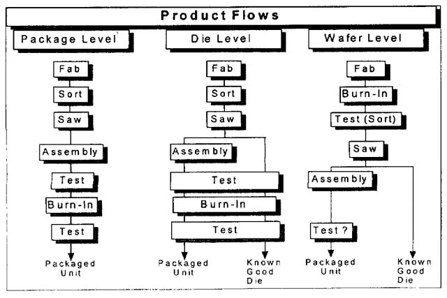
Fig. 4. Burn-in flow comparisons.
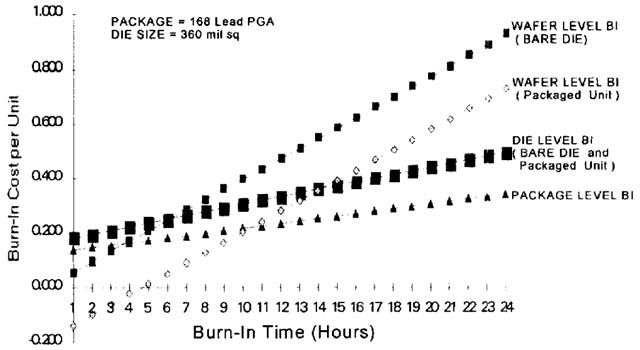
Fig. 5. Example of 'per Unit' cost model results.
The package level flow is what currently exists for component manufacturing and is provided as a reference point.
For the die level flow, the process will provide unpackaged (bare) die that have been burned-in and tested (i.e., KGD). From a process flow perspective, the KGD flow eliminates the assembly step, and uses the existing burn-in and test processes. As noted in the DLBI flow shown earlier, DLBI introduces some die & die carrier handling steps which in the end tends to make DLBI a more expensive process. Due to the different end use requirements, there will be two different product flows, depending on the desired configuration of the product (i.e., bare die or packaged).
For wafer level flow, one of the benefits to note is that the burn-in process step moves to much earlier in the product flow. Since the purpose of burn-in is to eliminate material with latent defects, the earlier in the process flow this occurs the better, because it prevents adding cost to a product that rejects later in the process. It also provides yield and defect data feedback sooner in the product flow enabling the factory to be more proactive in resolving problems [4]. A major implication is the need to make the wafer sort test step a full product performance test step, which also will be a major development effort, but would build on the whole wafer probe technology developed for WLBI. Another implication will be the need to improve the wafer saw process to eliminate defects introduced at that process step, as the ideal WLBI flow would have no further testing after wafer saw. For packaged product, there still may need to be some form of Post-Assembly Test Screen to eliminate defects introduced during the assembly process.
VII. BURN-IN METHODS COST ANALYSIS
Two types of cost models were developed, as tools, to better understand what process and equipment parameters have the greatest impact in developing a cost effective DLBI or WLBI Process. These models are the 'per unit' cost model and the 'total life spending' cost model. Basically, the cost models are a mathematical cost description of each process and its interactions. Cost models are a major subject in itself, so the building of cost models is not covered in this paper, however, some of the key points learned will be shared.
Some of the main parameters and assumptions used in both cost models were:
- Product volumes
- Wafer & die sizes
- Yields (e.g., die, assembly, BI, test)
- Burn-in process cycle times (e.g.. BI time, setup and takedown time, heat-up and cool-down time)
- Equipment utilization (e.g., idle time, scheduled and unscheduled downtime)
- Equipment and material costs (e.g.. BI boards, BI ovens, probe-heads, wafer station, die carriers)
- Facilities (e.g., floorspace, electricity)
- Labor & overhead
- Process induced damage and rework
It is very important to remember at this point in time, that both cost models are tools to better understand each of the burn-in processes under evaluation. It is much too early to use the cost models for making a GO/NO-GO type decision because many of the parameters and assumptions are only best estimates and will require validation. The real value of the different cost models at this point in time is to use them to identify, understand and focus on reducing the major cost contributors to the DLBI or WLBI system being developed. Once the prototype evaluation validates the different parameters and assumptions, then it is appropriate to start using the cost models to make GO/NO-GO decisions.
VIII. 'PER UNIT' COST MODEL
The 'per unit' burn-in cost model was the first to be developed. This detailed model allows making a 'snap shot in time' analysis based on a given set of parameters and assumptions.
The chart above shows an example of the modeled burn-in cost per unit (nominalized) versus burn-in time (hours). Burn-In time is used as one of the axis, because it acts as a cost multiplying effect, dependent on the slope of the line.
These results indicate that DLBI is about 30% more costly than the current PLBI, and may never be lower cost than PLBI due to the added process steps. It does indicate that DLBI would be an acceptable cost near-term solution for supplying KGD. The slope of the line for PLBI and DLBI is similar because they use the same basic process and equipment.
For WLBI, the slope of the line is much steeper than PLBI and DLBI, and this appears primarily driven by the cost of all the automated equipment. The per unit cost model does show that, under the lower burn-in times, WLBI can be significantly lower cost than the existing PLBI with the same basic conditions. The line for WLBI for a packaged unit goes below the zero cost line because the effects of the assembly and package savings are greater than the cost to do the Burn-in process step.
IX. 'PER UNIT' COST MODEL SENSITIVITY ANALYSIS
Since each cost model is a cost representation of the different process, the details of the cost model are proprietary, but we will discuss some of the basic results. One of the advantages of cost models is the ability to do cost sensitivity analysis by varying one or more of the parameter assumptions, with the result being a graphical characterization of the impact on the total cost. Using the WLBI 'per Unit' cost model, here are some good examples of the results and how usage of the cost models can help in the definition and development of WLBI.
As shown in Fig. 6, the product die size has a significant impact, because the smaller the die, the more die you get per wafer, which means the more potential good die that the costs are amortized across.

Fig. 6. Example of WLBI cost sensitivity versus die size.
The wafer yield has a similar impact as die size, as illustrated in Fig. 7. The higher the wafer yield, the more good die per wafer, the more potential good die that the costs are amortized across. High wafer yields for a small die size has a very significant impact on lowering 'per unit' cost.
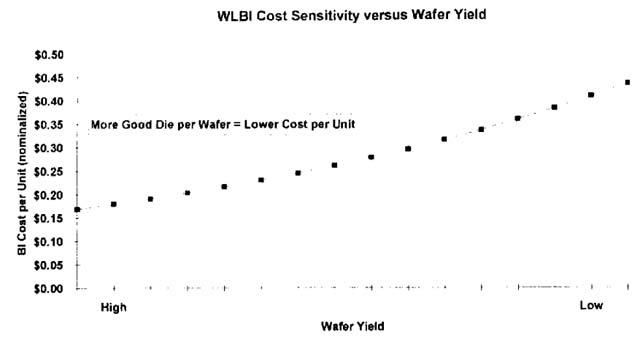
Fig. 7. Example of WLBI cost sensitivity versus wafer yield.
Fig. 8 shows that the higher the package or assembly costs, the more the savings, because screening the bad die before packaging prevents adding value to a product that will be scrap later in the manufacturing process. This results in a lower total process and product cost.
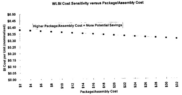
Fig. 8. Example of WLBI cost sensitivity versus package/assembly cost.
Comparing the cost sensitivity of the different equipment involved, in Fig. 9, indicates that where possible, it is better to share equipment across the whole system, even if it cost more to centralize it. A good example would be the wafer-to-probe alignment system. It would be better to install a more expensive unit on the central wafer handler than to install one at each station. From a cost per unit perspective, the cost of the shared equipment is spread across more good product, thus reduces the cost per unit.
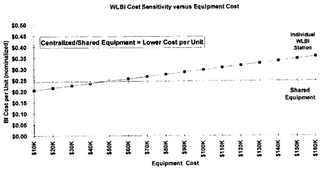
Fig. 9. Example of WLBI cost sensitivity versus equipment cost
The cost model sensitivity analysis indicated that WLBI was relatively insensitive to the following:
- Facility and utility costs.
- Reburn-in rates.
- Labor & overhead.
- Whole wafer probe card cost.
X. 'TOTAL LIFE SPENDING' COST MODEL
The burn-in 'total life spending' model was the second cost analysis model developed. This model looks at the total dollars spent to bum-in product over an extended period of time (e.g. seven years).
Shown Fig. 10 are the results of using the parameters and assumptions for three different microprocessor products in a new wafer fabrication facility. It shows that WLBI has a considerably higher start-up cost versus PLBI or DLBI. It also shows that the WLBI cumulative spending over time does end up being less than the cumulative spending for PLBI or DLBI. This model is also very sensitive to many of the key model parameters such as wafer yield, BI time, equipment costs and device packaging cost. Some of the key advantages of WLBI comes from cycle time reductions due to the inherent automation of the WLBI system. For WLBI, the high initial spending is due to the need to put enough capacity in place to support the total wafer fabrication volume, regardless of yield (i.e., good and bad die), whereas the PLBI and DLBI methods only have to have enough capacity to meet the sorted good die volumes. The potentially high startup costs of WLBI will require major development focus on equipment cost reduction, equipment centralization and utilization. The high startup costs of WLBI are a concern because the area under that part of the curve represents loss of opportunity (versus PLBI & DLBI) during that time for using that capital equipment money in other areas of the production process.
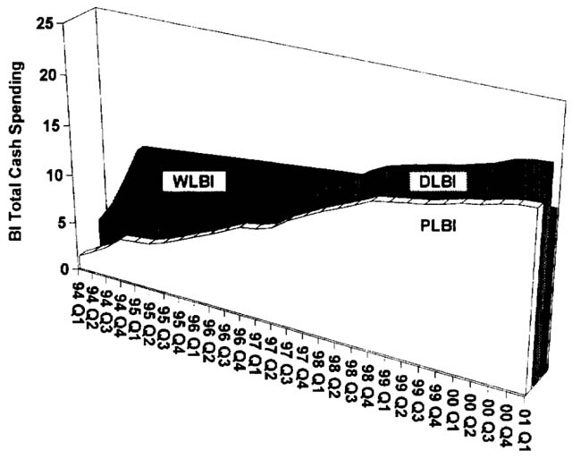
Fig. 10. Example of total cash spending model results.
Remember, that both cost models need valid parameters and assumptions before usage to make GO/NO-GO decisions.
XI. DLBI & WLBI DEVELOPMENT ROADMAP
Fig. 11 shows what is currently perceived by the industry to be the development roadmap for both DLBI and WLBI. The DLBI timeline is realistic and the WLBI is really a best case estimate with high risk of schedule slippage.
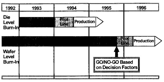
Fig. 11. DLBI and WLBI development timetable.
XII. CONCLUSION
New techniques of doing burn-in are necessary to meet the 'known good die (KGD) market demands of the multi-chip module (MCM) industry. In the near term, die level burn-in (DLBI) offers a cost-effective solution for supplying KGD. If significant reductions are to occur in burn-in process costs, further development of the burn-in technology is necessary, wafer level burn-in (WLBI) is potentially a good solution, however significant development is a requirement. Development of DLBI and investigation of WLBI, as well as other alternative burn-in methods, will need to continue.
ACKNOWLEDGMENT
Ken Reber and Vance Adams (both from Intel Corporation) are the two other people on the team that developed much of the data and pictures used in this paper. Ken Reber was responsible for identifying and evaluating the potential whole wafer probing technologies. Vance Adams was responsible for developing the cost models. The author would like to thank them for their significant contributions to the work reported in this paper.
REFERENCES
[1] 'Consortia for Known Good Die' report by Microelectronics and Computer Technology Corporation (MCC).
[2] Below is the list of manufacturers/developers identified as having potentially viable whole wafer probing technologies for development of a wafer level burn-in system. This is supplied to enable the reader to more easily contact them directly to get more details on their proprietary technologies.
- Elm Technology, Glen Leedy (contact person), 1061 E. Mountain Drive, Santa Barbara, CA 93108, (805) 969-0534.
- MicroModule Systems, Fariborz Agahdel (contact person), 10500 Ridgeview Court, Cupertino, CA 95014-0715 (408) 864-5960.
- nCHIP, David Tuckerman (contact person), 1971 North Capital Avenue San Jose, CA 95132 (408) 945-9992 (x237).
- Nitto Denko, Ron Blankenhorn (contact person), 55 Nicholson Lane, San Jose, CA 95134, (408) 432-5400 (x5422).
[3] Below is a list of some of the companies submitting proposals for the ARPA wafer level burn-in development per the ARPA BAA 93-25. This is supplied to enable the reader to more easily contact them directly to get more details on their proprietary technologies.
- Aehr Test Systems (ATS), Rhea Posedel (contact person), 1667 Plymouth Street, Mountain View, CA 94043, (415) 691-9400.
- Microelectronics and Computer Technology Corporation (MCC), Larry Gilg (contact person), 1200-A Technology Boulevard. Austin, TX 78727-6298, (512) 250-3044.
- nCHIP, David Tuckerman (contact person), 1971 North Capital Avenue, San Jose, CA 95132, (408) 945-9992 (x237)
[4] Barbara Vasquez et al., "Wafer Level Burn-In Can Accelerate Reliability Learning," Sematech Symposium on Applications Solutions for Known Good Die, Dec. 9, 1992.
David W. Gralian received the A.A. degree in electronics technology from American River College in Sacramento, CA in 197l.
He worked at Electronic Techniques. Inc. (1971-1973), Motorola Inc. (1973-1974) and Bowmar, Inc. (1974-1975). all in the Phoenix AZ area. He joined Intel Corporation in 1975. At Intel, he has managed the development of specialized test equipment. DRAM Product Assurance and i960 RISC Processor quality and reliability. He is currently the manager of the Intel Corporate Burn-In Technology Development group responsible for the continuous improvement and future development of the burn-in process.
Particle Interconnect - MMS - TI Known-Good-Die
Known-Good-Die probe/burn-in. Proof of removable die MCM-L/D/C.
Known Good Die: A Practical Solution
|
Randal Roebuck Texas Instruments M&C 7800 Banner Drive, MS 3936 Dallas, Tx 75251 (214) 917 - 6244 (214) 917 - 7391 Fax |
Fariborz Agahdel & Dr. Chung Ho MicroModule Systems™ 10500A Ridgeview Court Cupertino, Ca 95014-0736 (408) 864 - 7437 (408) 864 - 5950 Fax |
Known Good Die Interconnect System
The Semiconductor Industry is entering a new phase of packaging density with the development of electronic modules containing multiple integrated circuit (IC) die. A critical path, Known Good Die (KGD), has been identified in the development of muftichip modules. Semiconductor die, depending on their maturity and function, exhibit early life failures when tested across time. In order to sort out these eady catastrophic defects, the die are packaged and "burn-in conditioned at elevated temperatures. This prevents potentially defective devices from being placed in their final packaging scheme.
Texas Instruments (TI) and MicroModule Systems™ (MMS) have co-developed an interconnect system capable of burn-in testing individual die to a "Known Good Die" condition. TI and MMS have combined their expertise in component / system level designing, modeling, fabricating, and testing to offer this commercially available product. This interconnect product utilizes advanced thin film technology and fine pitch burn-in test sockets in conventional burn-in ovens avoiding excessive capital outlays. Key features include oxide penetrator of die's bond pads, die seif alignment, controlled impedance interconnect, universal burn-in testing hardware, and others. The system accommodates either standard aluminum or bumped IC pad configurations in area array or peripheral pad layouts. Also, it has the capability to test at high frequency, high densities, and high pin count.
Key Words: KGD INTERCONNECT SOCKET TEST BURN-IN
Objective: Test and Burn-in condition semiconductor devices using a socket / substrate interconnect system and die level testing methodology. Provide the capability to fully test and condition individual integrated circuits (die) without being packaged or tab taped with no destructive results.
Problem: The Semiconductor Industry is advancing fine line geometry technology in producing smaller and more powerful integrated circuits with testing becoming a limiting factor. Current mechanical test methods such as probe needles can not test the pad geometry features and speed requirements of these integrated circuits due to physical limitations. The devices must be integrated into the next level of packaging for test / conditioning.
The electronic market is driving semiconductor integrated circuits in performance and physical package size. Clock speeds, I/Os, and die / pad densities are increasing. Many of these integrated circuits are being packaged together into multi-chip modules (MCM) and hybrids to create high performance products. Th critical path driver for multi-chip module success is known as the term "Known Good Die". With many die mounted into MCM, the compound effect of yield becomes an issue. Either in a chips first or chips last assembly approach. die that have been fully tested and conditioned (burned-in) must be mounted in order to obtain optimal yields. The yield effects are shown in Figure 1.
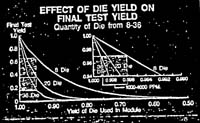
Figure 1. Effect of Die Loss on Final MCM's Test Yield
For example, twenty die assembled into a multi-chip module (MCM) having individual yields of ninety-five percent, will produce an MCM first pass test yield of 35%. Material scrap is undesirable and rework is very expensive and labor intensive. A method is needed to test and condition individual integrated circuit die (diced from the wafer) using existing manufacturing facilities so that IC's can be procured already tested and conditioned. This enabling technology will reduce material loss, improve assembly yields, reduce costly rework, and promote higher density interconnect methods of flip chip, chip-on-board, and chips first.
Current test methods are mechanical needles in wafer level probe and tab tape at the die level test. The mechanical probe needles have limited density capability and leave considerable damage on the bond pad. These impressions are unacceptable in the chips "first" MCM assembly approach.
Tab tape in higher density configurations is costly and requires circuit area for application to a packaging scheme. Flip chip enabled by a "Known Good Die" test methodology would offer 2X improvement over tab tape. Currently, U.S. sources of tab tape are limited.
Industry Need: Historically, product test flow in industry has been wafer level probe, package level testing / conditioning, and system level testing. Die level testing can be implemented before package level testing / conditioning and would maximize packaging scrap yields, reduce assembly rework, and improve product reliability. Die level testing is an enabling technology for both semiconductor and MCM manufacturers in low and high volume applications. An independent survey of 388 responses from various electronic professional society members was conducted in 1992. The survey indicated a high level of interest and sensitivity to cost of die level testing as shown in Figure 2.

Figure 2. Testing Applications and Features
The survey showed a significant amount of interest and need in the industry from all market sectors or package types. Interest levels have continued to rise since the survey.
Solution: A test method and product is being developed to meet the KGD requirements for both single chip and multi-chip module applications. TI and MMS have combined their expertise in component / system level finite element analysis modeling, CAD designing, fabricating, and testing, to produce a commercially available product. The technologies have been transitioned from a laboratory to a production capable environment with the product being useable in the present burn-in test environment without expensive capital investment.
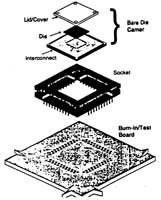
Figure 3. KGD Interconnect System
Hardware Description: The bare die lest and burn-in systems have been designed with several objectives in mind. First of all, it must meet functional specifications of electrical requirements in test and burn-in environments. The system has to be durable enough to withstand multiple usage through harsh test and burn-in environments. The other major criteria for such a system is its ability to make a temporary connection with the die without damaging the die pad area for any subsequent assembly operations. In addition, the assembly should lend itself for ease of automation and use with existing equipment.
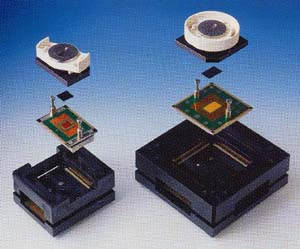
In the following sections, the hardware components are briefly described. As it is shown in Figures 3 & 4, the system is comprised of four major components, a substrate (interconnect), the holding and pressure assembly, a socket (system interface mechanism), and test or burn-in board.
Substrate's Interconnect Layer: The interconnect layer is used to make contact to the die pads, and fan-out the signals from the contact points to the socket. To achieve the electrical and functional spccifications of both AC/DC and functional test and burn-in systems, a multi-layer copper polyimide thin film interconnect mechanism was chosen. This allows the substrate to match the high pad density features of current and future products. The multi-layer structure also provides a controlled environment for high performance signals.
The interconnect layer must also be able to accommodate different die pad metallurgies such as aluminum, gold, and solder, in different shapes such as flat or raised.
Any contact configuration that could make electrical contact to standard Al pads could also accommodate the other types of pad configurations, since the contact point had to penetrate through the oxide layer formed on top of the aluminum.
Existing contact mechanisms accomplish this action by wiping away the oxide layer (as it is done with current probe cards). This wiping action invariably causes undesirable damage to the IC bond pad. A new technique was used to develop special contact points on the interconnect layer which would penetrate through the oxide layer without the need for a wiping action.
Due to the shape and the materials used in producing these contact points, as well as the non-planarity of the die surface, compliancy had to be built into the interconnect layers to accommodate the interface between the die and the interconnect layer non-planarities. To accomplish this, the hard substrate on which the interconnect layers are formed is removed from the area where the contact points are placed, leaving only the copper / polyimide interconnect, thus making a more compliant surface under the contact area. A frame of the substrate is left behind to hold the membrane area in its intended shape and form.
To further simplify the die holding assembly and assembly equipment and tooling, a fence structure is built on top of the interconnect layer which will hold the die aligned to the contact points using the die edges as its reference. This innovative alignment technique lends itself to low volume manual assembly and will easily accommodate vision die pick and place assembly equipment.
Holding and Pressure Assembly: The holding and pressure assembly holds the die and the interconnect together, while applying an appropriate amount of pressure to the interface. The assembly is made up of four major components (as shown in figure 4):
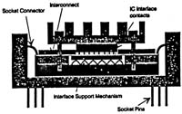
Figure 4. Holding and Pressure Assembly
I. The metal lid which holds the die in place, while pushing it toward the contact points on the interconnect layer. Being in intimate contact with backside of the die, the lid provides thermal management and can be designed to accommodate various heat dissipation requirements.
II. The inserts, which fit into the cavity formed by removing the substrate. The inserts perform two functions, to apply the appropriate pressure to the contact points, and accommodate any gross non-planarity between the die and the interconnect layer such as die thickness variations and assembly tolerances.
Ill. Backplate, which supports the inserts.
IV. Posts, which fastens the lid to the backplate.
The backplate, the insert and the substrate are supplied as a substrate assembly reducing the number of components required for final assembly. With this design the die would be placed on the subassembly, the lid positioned and fastened thus applying appropriate pressure to make contact between the die and interconnect layer.
Mechanical Analysis of Force: A contact force was used to make electrical connection between die to substrate. Ten grams force was used as the design parameter that is necessary to break through the aluminum oxide and make contact to the die's bond pad. In figure 5, the table shows the required forces needed for the number of bonding pads associated with a specific die.
| Bond Pads (#) | Force (lbs) |
| 55 | .59 |
| 160 | 1.73 |
| 235 | 2.54 |
| 340 | 3.68 |
| 520 | 5.62 |
Figure 5. Force Requirements
Thermal Analysis of Lid/Heat Sink: With each die user having different heat dissipation requirements, two different lids were designed to be used in the interconnect system. The design parameters were -55 ° C to 150 ° C environment and a 175 ° C "die" junction temperature. Assumption was made that all heat is dissipated through the lid. The standard lid is a 0.062" thick flat anodized aluminum plate. The special heat dissipating lid is the standard lid with multiple fins. The performance of each lid is shown in Figure 6.
| Lid Type | Surface Area (in2) | Rmax (° C/Watts) | Qmax (Watts at 150 ° C) |
| Standard-Flat Plate | 0.88 | 182 | 0.64 |
| Heak Sink Flat Plate-w/fins | 1.88 | 82 | 1.32 |
Figure 6. Thermal Dissipation of Lids
Socket (System Interface): The socket makes contact to the die carrier and transfers the signals from the pads on the interconnect layer to the destination system such as burn-in boards or tester board.
The existing socket is a modified 248 pin QFP socket which aligns the socket to the interconnect layer using three pins, which match three through holes on the substrate (interconnect / holding assembly). Final socket configuration will be determined using customer driven inputs.
Electrical Analysis of Socket / Substrate (Interconnect): The electrical analysis was completed using Maxwell Ansoft software for finite element analysis and PSPICE software for circuit analysis. The substrate (interconnect), socket, and socket / substrate system performance was analyzed and simulated for this report. The following issues were addressed: ground noise and power noise due to signal switching, impedance control for multi-layer and single layer thin film interconnects, socket ground / power / signal pin arrangement optimization, "dirty" versus "clean" power and ground separation, inductance, capacitance, and resistance parameter extraction.
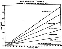
Figure 7. Noise Voltage versus Frequency
The limiting factor in the system was the top load socket normally used in burn-in functions for QFPs. It contributes 99% of ground noise and over 75% of power noise. With 200mV noise limit, one volt power, and 100 signals switching simultaneously, the substrate will meet the electrical performance specification at a maximum frequency of 263 Mhz, the socket at 17 Mhz, and substrate / socket at 16 Mhz. A custom KGD socket is being designed to increase the overall system performance to higher clock speeds. The following figure shows the relationship between the number of signals between grounds and system performance. To achieve optimal socket performance, the grounds should be located in middle row of the socket's through-pins and powers on the internal row, next to the grounds. This configuration allows ease of routing for the test / burn-in board designers using fine pitch high density sockets.
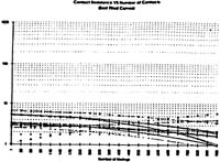
Figure 8. Contact Resistance versus Matings
Conclusion / Benefits: The Texas Instruments and MicroModule System™ burn-in test interconnect system will eliminate a variety of present test systems such as TAB tape, "softbond" wire bonding, and other test techniques which require valved [value] added processing.
Additionally, the contact system used will not introduce any significant pad degradations as is typical of other contact mechanisms such as probe needles. This will benefit specific MCM interconnect technologies such as chips first, as now a high quality bond pad attachment surface will be available.
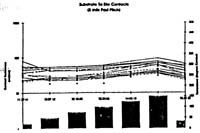
Figure 9. Substrate to Die Resistance
The TI/MMS approach to Known Good Die will enable the use of higher density die interconnect technologies such as flip chip (2x improvement over tab tape), chip-on-board, and chips first. This system will accommodate a variety of die configurations including flush bond pads, raised metallization, and bumped pads in either peripheral or area arrays.
The product can be readily used in a manual or automated assembly environment. By employing existing burn-in test equipment, large capital outlays can be avoided. Additionally, by supplying an open tooled socket family designed to enable a universal burn-in board, the cost of custom socket non-recurring and multiple burn-in board set up for various package types is eliminated.
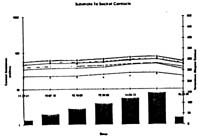
Figure 10. Socket to Substrate Resistance
TI/MMS KGD Interconnect System is being continually evaluated and further qualified. The results will be presented in subsequent papers and presentations.
Summary: The KGD Interconnect System provides dramatic influence on first pass MCM test yields and reclamation of single-chip package loss. It utilizes existing equipment and facilities and has comparable delivery and nonrecurring costs of present package-level methods. The flexibility of universal test and burn-in hardware provides the user better adaption to market conditions. The "Cost of Quality or Total Cost" and technology enhancements of the Known Good Die - Die Level Testing will be a significant contributor to the semiconductor and multi-chip module industries.
Acknowledgements:
U. Deshpande, MMS. Substrate Fabrication.
B. Griswold, MMS, Carrier Assembly & Test
D. Haedge, TI DSEG, Socket & Substrate Electrical Analysis of KGD Interconnect System Report.
J. Heimann, TI M&C, KGD Program Manager, and Editor
S. Husain, MMS, Mechanical Design & Modeling.
P. Lavault, TI M&C, Testing.
S. Rizzo, TI M&C, System Testing & Qualification.
S. Subramanyam, TI M&C, Baseline Thermal Transfer Analysis of KGD Lid Report.
S. Westbrook, MMS, Substrate Design.