Comparing Socket Technologies
- Particle Interconnect
- IBM dendrite
- Metal spring
- Conductive elastomer
- Fuzz button
- Pogo pins
- Side contact
- Micro-machined silicon probe card
- Connector manufacturers
Particle Interconnect
Particle Interconnect performance
- Temporary, or permanent contact even in presence of adhesive, grease, or solder.
- Gas-tight oxide-penetrating connection.
- Plastic deformation of contact mating surface.
- Minimal surface disturbance.
- Independent of common electronic metals.
- Simple mechanical connection and trace design.
- Temperature range used: > 450° to -270° C.
- Minimum interconnect dimensions: 6 μ, pad 12 μ pitch.
- Attached dies passed four cycles of Mil-Std-883C (burn-in, thermal shock, pressure, salt/fog corrosion) test without any damage.
- Life test: at 30 gram-force produced 3 - 5 milli-Ohms contact resistance even after 1,500,000 insertions.
- Contact force & resistance:
- 10 gram-force, 10 milli-Ohms of resistance,
- 50 gram-force, 3 milli-Ohms of resistance.
- Current carrying capability: 0.020"2 pad at 9 gram-force has > 12 amps.
- Vertical axis contact length (signal integrity requires small size): 0.001".
- Vertical axis compliance (accomodating non-planar dies): > 0.040" (depending on design).
- Method for penetrating the oxide of package lead: sharp small diamond particles with no scrubbing for durability, compared to metal scrubbing or metal penetrating contacts.
- Controlled impedance: 50 Ω ± 1 Ω to the lead of package (Typical design capacitance & inductance: < 0.001 pF & < 0.01 nH).
- Bandwith tested to > 65 GHz (for high-speed and radio-frequency applications).
- All steps of electronic product development: prototyping, test (controlled impedance), burn-in, emulation/characterization, field replacable, and production.
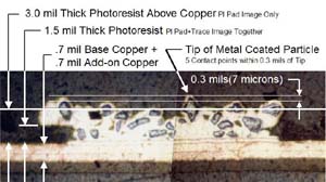
Particle Interconnect planarity and accuracy
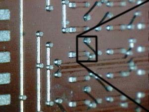
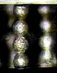
Current planarity of pads and accuracy of alignment of particles on pads.
 |
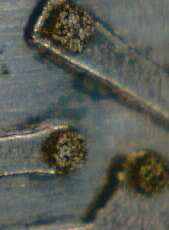 |
| PCB traces with pads | Close up |
Note sharp corners of the particles that make electrical contact at very low pressure to form a temparory bond. Solder would wick into spaces between the particles during reflowing to form perament bond.
 |
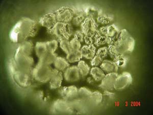 |
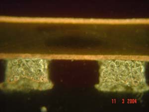
| Cross-section of the PI pad shows planarity of a single pad as well as planarity to adjacent pad. | Close-up of PI pads shows controlled stacking of particles to a desired height with clearance between individual particles. |
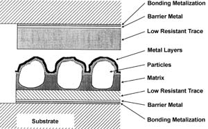
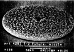
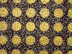
Cross-section of Particle Interconnect pad
Demonstrates uniformity & planarity of particle protrusion above photoresist.
- 0.020" diameter x 0.003" tall nickel Particle Interconnect pad on 1 oz copper.
- Using 25 micron particles. Planarity of 1/2 particle diameter.
 |
 |
Picture courtesy of Larry DiFrancesco.
Texas Instruments DieMate™
Burn-In Test Sockets for Chip Scale Packages: Overcoming the Challenges of Fine Pitch BGA
Updated July 19, 2004
Written in 1998 By James A. Forster, Kiyokazu Ikeya, Masao Tohyama and Sal P. Rizzo
Texas Instruments Incorporated, Mansfield, MA
...
Low Inductance: <4nH
Higher inductance: 5 to 13 nH... The Future
The need for a cost effective solution for packages with pitches less than 0.75mm has been identified by a number of customers. A number of techniques are available today but these are not considered cost effective and are not easily adapted to use in the installed base of high volume handling and processing equipment. In general these techniques are extensions of carriers developed for testing bare die.
Contact Pads on Flex Membranes
TI's DieMate product with a flexible membrane manufactured by MMS is shown in figure 10. This technology is currently being evaluated for use in CSP's.
...
- Ability to contact aluminum, solder bumped, or gold bond pads
in area array or peripheral configurations - Impedance control for high speed functional test
- Lowest cost, most reliable system: -- Test costs as little as $0.25
- Proprietary contact system [Particle Interconnect] does not degrade die pads
-- 500 cycle test life
Connect2it
PI-Exatron licensee since 1991
Connect2it Diamond Particle Interconnect Product Information
 Photo courtesy of
Connect2it.
Diamond Particle Interconnect (DPI) technology begins with individually metallized diamond crystals screened at levels between 10 and 50 microns. These diamond particles are selectivelyelectroplated onto the substrate traces using standard photoresist process.
DPI creates a "micro bed-of-nails" that makes electrical contact through penetration of oxides, rather than the traditional wiping action of standard contactors. The DUT is pressed onto theDPI "bed-of-nails" which pierces the surface oxidation on the device lead and forms a gas tight seal. Typical particle penetration is approximately 5 to 10 microns. The DPI interconnect has the electrical integrity of a solder joint as demonstrated with TDR data or side-by-side comparison. Contact resistance is extremely low, approximately 3 milli-Ohms.
There are numerous benefits to using DPI technology. Lead coplanarity is maintained with successful contact at approximately 10-12 grams/lead. In addition to signal and lead planarity integrity, DPI offers an extremely long lived test environment. When properly implemented and conforming to the manufacturers DPI mechanical design rules, contacts last over 4 million insertions. Contacts can be readily reconditioned to remove contaminants through a simple reflow procedure with flux and a solder iron.
Chip Scale Review Online
Reach for the Sky! As Socket Choices Multiply in the GHz Range, Makers Face New Demands
April 2003
By Ron Iscoff, Editor
...
In addition to the usual test complexity of lower-frequency sockets, high-frequency units add such issues as compliance, parasitics and crosstalk.
Socket Technology
Other considerations common to the short or coaxial probe technology employed for many high-frequency sockets include impedance, bandwidth, self-inductance, capacitance and insertion loss (see glossary).
...
Figure 3. Exatron offers Particle Interconnect test sockets. The sockets employ metallized diamond particles to form a micro "bed-of-nails" contact. The rough surface created by PI allows for zero lead length interconnect of DUT leads and testboard circuits, ideal for RF testing, the company says. The resulting contact offers a resistance of less than 3 ... [milli-Ohm].
...
Until wafer-level burn-in becomes a reality, the emerging multi-chip packaging industry needs practical solutions that screen for reliability and performance.
By Dr. Tom Di Stefano,Centipede Systems, San Jose
CSPs and their wafer-level cousins face increased demands for performance and reliability driven by the boom in multi-chip packaging.
Early stacked CSPs were rather simple affairs aimed at cell phones and personal electronics. As multi-chip packaging extends into critical applications, test requirements are becoming more demanding.
The known-good die (KGD) problems that plagued MCMs a decade ago have resurfaced with increasingly complex system-in-package configurations. Whether in wafer-level or bare-die form, the chips must be tested for speed and reliability before assembly in the more complex systems.
...
One attractive approach is the testing of whole strips or trays of CSP or WLP chips during thermal stress.
...
- CSP: Chip Scale Packaging
- WLP: Wafer-Level Packaging
IBM dendrite
IBM DendriPlate™
Contact pad has numerous hard dendritic spikes made of electroplated palladium that provide a relatively large contact area. Planarity is hard to control. It has limited contact life (about 10 remates), and contact resistance increases due to dulling of dendrites after each remate.
BGA Sockets - A Dendritic Solution
Benson Chan, IBM Corporation, Endicott, New York, 13760
Pratap Singh, RAMP Labs, Round Rock, Texas, 78681
1996 IEEE Electronic Components and Technology Conference
Abstract
Today's high density technology requires a large number of I/O pins in CPU packages. The direct soldering of these devices can lead to solder joint reliability concerns. ... sockets can provide a cost-effective solution in such applications when it comes to equipment upgrades and reducing the rework cost of CPU replacement. ... sockets allow the mother boards to be assembled off shore and imported with low tariffs. The CPUs can then be inserted on the planar according to the demands of US market. This paper compares the current BGA socket technology and describes a low profile BGA/LGA socket based on dendrite technology developed by IBM Microelectronics Division.
...
Table 4. Dendrite Contact Electrical Characteristics
Bulk Resistance 0.587 milliohms Capacitance 0.032 pF Inductance 0.0097 nH Normal force, minimum 30 grams per contact Table 5. Dendrite Contact Physical Characteristics
Pad Size .028 inch Via Size .004 to .014 inch Cross section 2 S Base material Polyimide or FR4 Contact pad pitch .050 x .050 to .020 x .020 Overall Thickness .010 inch ...
Flexible Printed Circuit Attachment Method
By Derek Schultz
Metal spring
Contact compliance is provided by bending of metal.
IBM ELASTICON connector
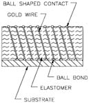
A new direction for elastomeric connectors
B. Beaman, D.Y. Shih, G. Walker
Enterprise Syst. Div., IBM Corp., Poughkeepsie, NY
Proceedings of the 43rd Electronic Components and Technology Conference, 1993.
... Multichip modules are one of the many applications that benefit from the high density interconnection capabilities of elastomeric connectors. The ELASTICON connector is a new high performance elastomeric connector that was developed to address some of the key limitations of existing MCM and land grid array connectors. The ELASTICON connector uses gold or gold alloy wires for the conductive elements embedded in an elastomer material. ...
InterCon Systems cLGA ®
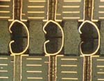 Photo courtesy of Mark Plucinski, IBM Rochester.
"C" shape electroplated BeCu spring contacts are inserted into plastic housing. Spring protrudes slightly above each surface, and require an exact amount of compressive force (for structural deformation and stability) to become flush with housing. To make it commercially practical, they require simple and compact alignment and actuation.
- Contact resistance: 20 milli-Ohms maximum initial, 10 milli-Ohms maximum change per contact after test, at 50 gram-force full deflection
- Inductance: < 0.2 nH mutual
- Capacitance: < 0.02 pf mutual
- Durability: 100 mating cycles
- Operating frequency at 1dB loss: 7.3 GHz at 2:1 signal to ground ratio
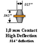
InterCon Systems C-Byte™
 Photo courtesy of InterCon Systems.
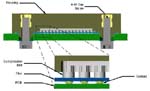 Photo courtesy of InterCon Systems.
C-Byte™ high speed flex compression system
... uses preformed brass contacts that are gold over nickel plated. ...
A molded thermoplastic housing provides mechanical support, and a compression mat exerts individual contact normal force when terminated to board. ... Mating circuit boards require only an array of plated contact pads. No mating connector is required. Only two screws must be secured to terminate the connector to board.
...
- Contact height: 0.010"
- Durability: 250 mating cycles
Conductive elastomer
Conductive metal partially embedded in an elastomer by molding. It requires careful control of the material properties for long-term temperature-dependent creep and stress relaxation, and molding parameters.
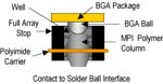
Metallized Particle Interconnect
 Photos courtesy of Tyco.
Tyco Electronics MPI - PRODUCT SPECS
- Contact resistance: 50 milli-Ohms max at 60 grams/column average
- Inductance: <0.40 nH at 1.0 kHz
- Capacitance: <0.01pF and 1 MHZ
- Durability: 20 mating cycles
- Current rating: 4 amps per column max.
Paricon Pariposer®
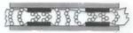 Applied load 40%.
 Photos courtesy of Paricon.
Subject: Capability of PariPoser® Contactor System
... The PariPoser interconnection system is comprised of highly organized conductive columns of spherical particles supported in an elastomeric matrix (Photo 1). These columns provide a compliant interconnect between opposing pad layers. Multiple columns are provided for each interconnect to provide a high level of redundancy (Photo 1). Unlike wire based elastomer interconnection systems, the PariPoser interconnect does not take a set due to the classic phenomena known as Euler column failure. As a result it is capable of high cycle life and will not be damaged by short term overloading. The PariPoser system is application engineered to meet the project requirements. Products designed for a pitch ranging from 1mm to chip scale have been provided. Custom designs including shorting contacts have also been developed. The thickness of the PariPoser fabric is between 0.006" and 0.020" with the thinner material providing better electrical performance.
... impedance of ~ 55 ohms and a loss of ~ 1 dB at 40 GHz. ...
- Contact resistance: 6 - 11 milli-Ohms at 50 psi (36 gram-force per contact)
after 1100 hours of thermal cycling - Current rating: 3 amps resulting in 75° C temperature rise
Fujipoly
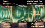 Photo courtesy of Fujipoly.
Fujipoly America - Zebra® elastomeric connectors W Series
... 300 to 2,000 fine metal wires per cm2 are embedded vertically in a transparent silicone rubber sheet. ...
- Contact resistance: 250 milli-Ohms at 90 gram-force
- Current rating: 0.5 mm thick sheet has 500 mA/mm2
Shin-Etsu Polymer
Shin-Etsu Polymer Co., Ltd. Antisotropic conductive sheet MT-P Type
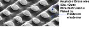
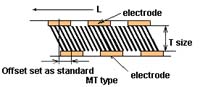 Photo courtesy of Shin-Etsu.
...
Tip of wire is protruded from the base elastomer for 20um and Ni/Au plating was done to improve contact.
...
- Contact resistance: about 100 milli-Ohms at 200 gram-force/mm2
Fuzz button
 Photo courtesy of Michael Griffen, IBM East Fishkill.
A column (fuzz button) of kinked molybdenum or BeCu wire (electroplated with a noble metal) in a cylinder. The contact looks like steel wool pad. The column can be compressed elastically over a relatively large axial displacement. Fuzz button interposer has small holes with a fuzz button inside each hole that projects both above and below the the interposer.
The contact range of motion is significantly larger than dendritic connectors, while the contact force is comparable.
Austin Spring Workshop of the System Packaging Committee
... co-planarity has proved to be VERY important - co-planarity must be better that 0.006 inches.
But Unisys abandoned CINCH and went to a Thomas & Betts [Purchased by Tyco] metallized polymer socket. The problem was that some of the fuzz buttons fell out of the via holes. If the assembly floor is carpeted, the operators had to search the floor for fuzz buttons, AND THEN TRY TO FIND THE VIA HOLE THAT HAD LOST THE BUTTON! (Very time-consuming)
...
Cinch
 Photo courtesy of Cinch.
- Contact resistance: 20 milli-Ohms at 2.5 ounces (71 grams)
- Contact height: 0.8 mm (0.032")
- Button diameter: 0.020"
- Inductance: < 1 nH
- Durability: 25,000 Z-axis actuations (CIN::APSE contact only)
- Current rating: Up to 3 Amps
Pogo pins
Interconnect Devices, Inc.
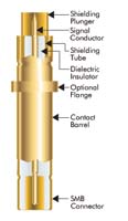 Photo courtesy of IDI.
... Coax probes are us.
We quickly became the primary source for coaxial designs. As we worked with literally hundreds of test engineers to develop new solutions, our design options grew exponentially. Simply, for you this means there should already be a probe in our line that will match your application. This catalog offers 11 off-the-shelf coaxial probes, with 3 new designs introduced with this catalog. Our special Coax Catalog has over 50 additional, build-to-order designs. If your application requires a custom designed probe, we're the people who can design and build it.
...
- Contact resistance: 50 milli-Ohms at 1.1 ounce (31.2 grams)
- Inductance: 0.93 nH
- Capacitance: 0.08 pF
- Durability: > 500,000 cycles
- Current rating: 3 amps continuous
Side contact
Plastronics
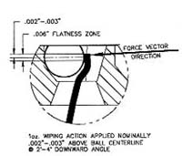 Photo courtesy of Plastronics.
...
Contact on upper hemisphere of the solder ball
Plastronics' patented contact touches and 'wipes' the solder ball on the upper hemisphere, eliminating the possibility of unacceptable solder ball deformation and related problems in package solderability. Patent No. 5,419,710.
...
- Contact resistance: 50 milli-Ohms at 10 gram-force
- Inductance: < 6 nH
- Capacitance: < 2.59 pF
- Durability: 10,000 mating cycles
- Current rating: 1A
- 1 oz. wiping action applied 0.002" - 0.003" above ball centerline, 2-4° downward angle
Micro-machined silicon probe card
Micro-Machined Array Probe Card
A membrane probe card designed for high speed, high pin count testing has been fabricated with conventional IC technology on a silicon wafer and its functionality demonstrated. A novel method of breaking down interfacial oxide, as a replacement for mechanical scrubbing, is proposed and demonstrated....
- Contact resistance: 2000 milli-Ohms at 10 psi
- Contact height: 0.001"
- Partially controlled impedance
- Durability: 1000 cycle
- Current rating: 50 milliamps