Reducing Cray form factor using Particle Interconnect
Particle Interconnect enabled the repackaging of the Cray J90 vector processor by increasing connector density 100 times while maintaining ultrahigh speed signal integrity. It achieves 75% weight reduction and 80% volume reduction over the commercial CRAY J90 supercomputer. However, had they used the proven Removable Die Multichip Module with the proven microchannel heat exchanger, and stacked these in a 3D fashion; they could have gotten the closest 3D packing of the dies and reduced the communication latency to the bare minimum.
The smallest latency (minimum wiring distance) would be achieved by placing memory die on one side of the interposer and the processor on the opposite side of the same interposer in a face-to-face configuration. This assumes the pin-out of the memory die matches the processor pin-out correctly. Since pin-outs usually don't match in that fashion; a microchannel heat exchanger, memory die, interposer, rerouting board (memory controller), interposer, processor die, and microchannel heat exchanger format would probably be the proper configuration. A one mm thick microchannel heat exchanger; which has been demonstrated to remove 5,000 W/cm2; would act as the clamps that hold everything together. The excess cooling capacity results in 2 fold increase in reliability for each 10° C temperature drop.
Particle Interconnect blind vias unlike drilled holes/buried-blind vias do not reduce routing area or yield. Therefore, they can reduce layer count.
The ability to replace any die, interposer, or rerouting board in the field would allow easier maintenance and upgradeability, dramatically reducing the logistical support.
Repackaging of a Cray Research J90 vector processor
Advanced System Packaging For Embedded High Performance Computing
|
Ken Sienski E-Systems, Garland Division ... |
Candy Culhane National Security Agency ... |
Abstract
Recent advances in microelectronic packaging promise unprecedented levels of performance for embedded computing. High performance machines that have been traditionally confined to a computer room environment can now be packaged for airborne, shipborne, or mobile applications. Multichip module (MCM) packaging has emerged as the first step in achieving this level of integration. However, new technologies are also required to provide the systems infrastructure needed to support high power density assemblies in an embedded environment. This paper outlines an approach that leverages recent advances in system packaging to meet modern challenges in high density interconnect, thermal management, and power distribution.
Introduction
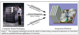
Figure 1 illustrates the repackaging of a Cray Research J90 vector processor from a traditional computer room enclosure to an "integration platform" suitable for an embedded environment. The J90 architecture scales in four processor increments from a minimum four node configuration (800 MFLOPS) to a maximum of thirty-two nodes (6.4 GFLOPS). The repackaged unit shown in figure 1 consists of four "system elements," each comprising a four node building block, for a total performance of 3.2 GFLOPS. This level of miniaturization is achieved through the application of multichip module and 3-D memory stacking technology. The integration platform also provides the necessary high density interconnect, cooling, and power distribution. The complete unit is sized to fit in a standard 19 inch rack.
The infrastructure components of the integration platform can be applied to a broad class of systems. Each system element is a self-contained unit that exhibits the following characteristics:
| Board Area: | 125 in2 (double sided) |
| Power Dissipation: | 500 Watts (3.3 Vdc) |
| Signal Interconnects: | 4000 |
This model applies to a wide variety of commercial architectures including signal processors, general purpose multiprocessors, and scalable computers. Although not every architecture will exhibit all of these characteristics, the system packaging concept will accommodate all dimensions simultaneously.
High Density Interconnect
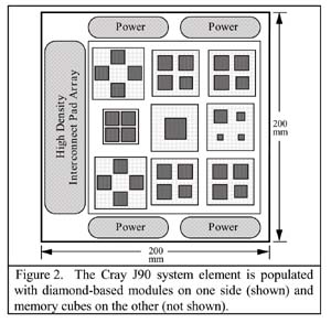
At the core of the system element is a double-sided printed circuit board fully populated with multichip modules. Figure 2 illustrates the processor side of the Cray J90 system element. An array of pads is provided on the left side of the card for external signal I/O. Large contact pads are also provided for power supply at the top and bottom edges. The required routing density is achieved through advanced printed circuit board technology capable of employing up to 52 layers.
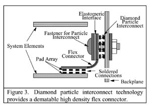
The communication bandwidth of the system element requires a departure from the traditional "edge connector" for signal interconnect. Instead, a flex connector is soldered directly to a high density array of interconnect pads on the surface of the card. A dematable attach mechanism between the flex connect and integration platform backplane allows removal of a single system element. As shown in figure 3, diamond particle interconnect technology provides this capability with a reliable contact mechanism.
Thermal Management
The thermal management problem produced by the density of the system element is addressed on two fronts. First, synthetic diamond material is employed as the MCM substrate to provide an isothermal surface for efficient thermal conduction from the individual die[1][2]. Then with the modules mounted in a "flipchip" style attach, the back of the diamond substrate is available for heat removal using a novel spray cooling technique [3]. A mist of Flourinert® created by spray nozzles located at the edge of the board produces a phase change from liquid to gas as the fluid comes in contact with the hot diamond surface.
Synthetic Diamond MCM Substrates
Table 1 compares the thermal conductivity of synthetic diamond with other common packaging materials. There are three characteristics of diamond that make it an ideal choice for an MCM substrate; high thermal conductivity (1500 W/mK), coefficient of thermal expansion (1.5) close to silicon, and properties of an electrical insulator [4][5].
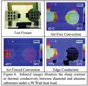
Diamond substrates provide an effective mechanism for distributing heat load from a point source produced by high power chips in an MCM application. Figure 4 illustrates the contrast between the thermal performance of a diamond and aluminum oxide (alumina) substrate under an equivalent heat load. The two substrates are compared in three different environments; air-free convection, air-forced convection, and edge conduction. As shown in the figure, the diamond substrate maintains a lower temperature under all three conditions. The edge conduction example provides the most dramatic example of heat transfer with a single ice cube applied to the edge of both substrates.
| Table 1. Synthetic diamond offers superior thermal conductivity over common substrate materials. | ||
| Material Conductor (C) Semiconductor (S) Insulator (I) | Thermal Expansion (ppm/°C) | Thermal Conductivity (W/m°C) |
| CVD Diamond (I) | 1.5 | 1500 |
| BeO (I) | 6.4 | 223 |
| AlN (I) | 3.3 | 170 |
| Alumina (I) | 6.3 | 29.3 |
| Polyimide (I) | 50 | 0.2 |
| Silicon (S) | 2.6 | 149 |
| Kovar (C) | 5.9 | 17 |
| Copper (C) | 16.8 | 395 |
| Silver (C) | 19.6 | 428 |
| Aluminum (C) | 23.8 | 237 |
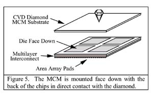
As shown in figure 5, a conventional "chips first" process is used to fabricate the diamond substrate MCM. The comparable coefficient of thermal expansion between diamond and silicon allows direct attachment of the die to the substrate for maximum heat transfer. The multilayer interconnect is constructed over the surface of the devices, providing electrical contact without wirebonds. The final assembly is mounted face down on the printed circuit board using an area array attach mechanism to provide the required number of contacts.
Spray Cooling
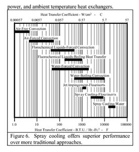
Spray cooling is used to remove the heat from the exposed surface of the diamond substrate. The graph in figure 6 compares the heat transfer efficiency of several common cooling techniques. Spray cooling can achieve a heat transfer coefficient two orders of magnitude greater than the air-forced convection used in most office computer equipment. It is even an order of magnitude better than the liquid-forced convection popular in more sophisticated electronics. This improved efficiency results in smaller coolers, lower flow rates, less pumping power, and ambient temperature heat exchangers.
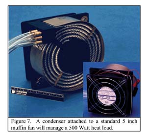
A phase change process is sustained by continuously coating the diamond surface with a uniform thin film of Flourinert®, the preferred heat transfer fluid. This is accomplished by replenishing the fluid with a fine spray as it evaporates. A clamshell enclosure is used to house the system element electronics in a sealed chamber with spray nozzles directed laterally across the substrates. The vapor is returned to an external condenser to complete the closed-loop system. The heat exchanger used to condense the Flourinert® exploits existing components to reduce cost and minimize impact to the system. Figure 7 illustrates a 500 Watt heat exchanger integrated with a standard 5 inch muffin fan. The fluid pump is located in the hub of the condenser coils.
Power Distribution
Low voltage, high current power distribution to each system element will create parasitic reactances that degrade power quality. This condition could be greatly improved through a new approach that distributes power at high voltage and provides conversion close to the point of load. Existing power converter technology is thermally limited and cannot be miniaturized due to the method of power semiconductor packaging and cooling. Spray cooling can be applied in this application to improve power converter efficiency from a typical 50 W/in3 to over 1000 W/in3.
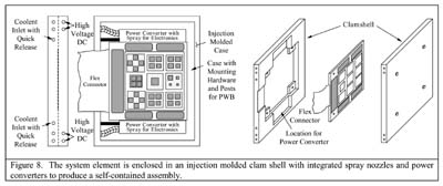
A conventional 800 Watt dc/dc power converter will occupy approximately 16 in3. Addition of a heat sink will at least double the size. Bulky power converters are difficult to locate near the point of load as required. In contrast, a spray cooled 800 Watt dc/dc converter will occupy only 0.3 in3. A component this small can be mounted directly on the printed circuit board. Figure 8 illustrates the integration of spray cooled dc/dc power converters within the system element clamshell. Connecting the clamshell to the heat exchanger in figure 7 results in a completely self-contained assembly.
Acknowledgment
Development of the J90 system element and integration platform is sponsored by the National Security Agency (NSA) under the High Performance Computing with Diamond Based Technologies program (contract MDA904-94-C-6210). The authors wish to express special appreciation to Mr. Paul Boudreaux for his continued support as a government program monitor. The authors would also like to acknowledge the many technical contributions of team members from Cray Research, Diamonex, Isothermal Systems Research (ISR), and Norton Diamond Film.
References
[1] Richard C. Eden, "Application of Bulk Synthetic Diamond for High Heat Flux Thermal Management," 1997 SPIE High Heat flux Engineering II, July 12-13, 1993
[2] Richard C. Eden, "Application of Synthetic Diamond Substrates for Thermal Management of high Performance Electronic Multi-Chip Modules," Applications of diamond Films and Related Materials, Y. Tzeng, M. Yoshikawa, M. Murakawa, and A. Feldman, eds. (Elsevier Science Publishers B.V., Amsterdam, 1991)
[3] Donald E. Tilton, Charles L. Tilton and Martin R. Pais, "High-Flux Spray Cooling in a Simulated Multichip Module," Topics in Heat Transfer Volume 2, ASME HTD-Vol.206-2, 1991
[4] T. J. Moravec, R. C. Eden and D. A. Schaefer, "The Use of Diamond Substrates for Implementing 3-D MCMs," 1993 Proceedings International Conference on Multichip Modules, April 14-16, 1993
[5] D. A. Schaefer, R. C. Eden and T. J. Moravec, "The Role of Diamond in 3-D MCMs," 1993 Proceedings of NEPCON '93, February 11-14, 1993
Airborne Demonstration of a Miniaturized Commercial Supercomputer
|
Ken Sienski Red River Engineering ... |
George Wos Cray Research ... |
Al Dieringer Raytheon E-Systems ... |
Candace Culhane National Security Agency ... |
Paul Boudreaux Lab for Physical Sciences ... |
Paul J. Boudreaux, Richard C. Eden
3-D Electronic Interconnect Packaging
|
Ken Sienski E-Systems, Garland Division ... |
Richard Eden Technology Applications ... |
Dean Schaefer E-Systems, Garland Division ... |
| Table 1. Size and Weight Comparison | |||
| Parameter | 6U VME | 3-D MCM | Reduction |
| Single Element Weight | 560 g | 20 g | 28: 1 |
| Support Structure Weight/Element | 800 g | 170 g | 4.7:l |
| Single Element Volume | 650 cm3 | 26 cm3 | 25:1 |
| Active Die Area/Element | 32 cm2 | 16 cm2 | 2:1 |
...
| Table 2. Bandwidth and Thermal Performance Comparison | |||
| Parameter | 6U VME | 3-D MCM | Increase |
| Layer-to-Layer Connections | 192 | 2500 | 1:13 |
| External Connections/Layer | 200 | 400 | 1:2 |
| Maximum Power | 50 W | 500 W | 1:10 |
| Layer-to-Layer Data Rate | 150 MHz | 1 GHz | 1:6.7 |
...